Electroluminescent Display

a technology of electroluminescent display and pixel, applied in the direction of electrical equipment, semiconductor devices, instruments, etc., can solve the problems of non-uniformity of pixels, differences in driving characteristics between pixels, and inability to obtain uniform image quality of electroluminescent display, etc., to achieve uniform image quality, reduce power consumption, and high potential driving voltage

Active Publication Date: 2018-07-05
LG DISPLAY CO LTD
View PDF1 Cites 51 Cited by
  • Summary
  • Abstract
  • Description
  • Claims
  • Application Information

AI Technical Summary

Benefits of technology

[0012]An electroluminescent display according to the present disclosure includes a display panel including a plurality of pixels, each of the plurality of pixels including subpixels. A pixel circuit of each subpixel includes a driving transistor connected to an anode of an electroluminescent diode, the driving transistor and configured to drive the electroluminescent diode, a first switching transistor connected to the driving transistor, the first switching transistor configured to supply a first voltage to a gate electrode of the driving transistor in response to a first scan signal, a second switching transistor connected to the driving transistor, the second switching transistor configured to supply a second voltage to the gate electrode of the driving transistor in response to a second scan signal, a third switching transistor connected to the second switching transistor and the driving transistor, the third switching transistor configured to supply the second voltage to a first electrode of the driving transistor in response to the second scan signal, a fourth switching transistor connected to the driving transistor, the fourth switching transistor configured to supply a first supply voltage to a second electrode of the driving transistor in response to an emission control signal, a first capacitor connected between a first node that is connected to the gate electrode of the driving transistor and a second node that is connected to the second electrode of the driving transistor, and a second capacitor connected between the second node and a power supply line supplied with the second voltage or the first supply voltage. A second supply voltage is applied to a cathode of the electroluminescent diode, the second supply voltage lower than the first supply voltage Thus, the electroluminescent display according to the present disclosure can implement uniform image quality over the entire screen without designing VDD lines at a low resistance and can reduce power consumption because the high potential driving voltage and a reference voltage are not short-circuited.
[0013]An electroluminescent display according to the present disclosure includes a display panel including a plurality of pixels each of the plurality of pixels including subpixels. A pixel circuit of each subpixel includes a driving transistor connected to an anode of an electroluminescent diode, the driving transistor configured to drive the electroluminescent diode, a switching circuit configured to supply a reference voltage that is less than a first supply voltage and greater than a second supply voltage that is less than the first supply voltage to a gate electrode and a first electrode of the driving transistor in response to a (n−1)th scan signal, the switching circuit configured to supply a data voltage to the gate electrode of the driving transistor in response to an nth scan signal, and the switching circuit configured to supply the first supply voltage to a second electrode of the driving transistor in response to an emission control signal, where n is a positive integer, a first capacitor connected

Problems solved by technology

However, there may be a difference in the driving characteristics between the pixels by various causes including a process variation, etc.
As a result, non-uniformity of the pixels is caused.
Hence, an electroluminescent display cannot obtain the uniform image quality.
However, because a width of a VDD line in a high resolution display panel needs to be narrowed and a length of the VDD line needs to be long, there is a limit to improving the voltage drop of the VDD using a method of reducing a VDD resistance in a large-screen display panel with high resolution.
Such a short-circuit current results

Method used


Image

  • Electroluminescent Display
  • Electroluminescent Display
  • Electroluminescent Display

Examples


Embodiment Construction

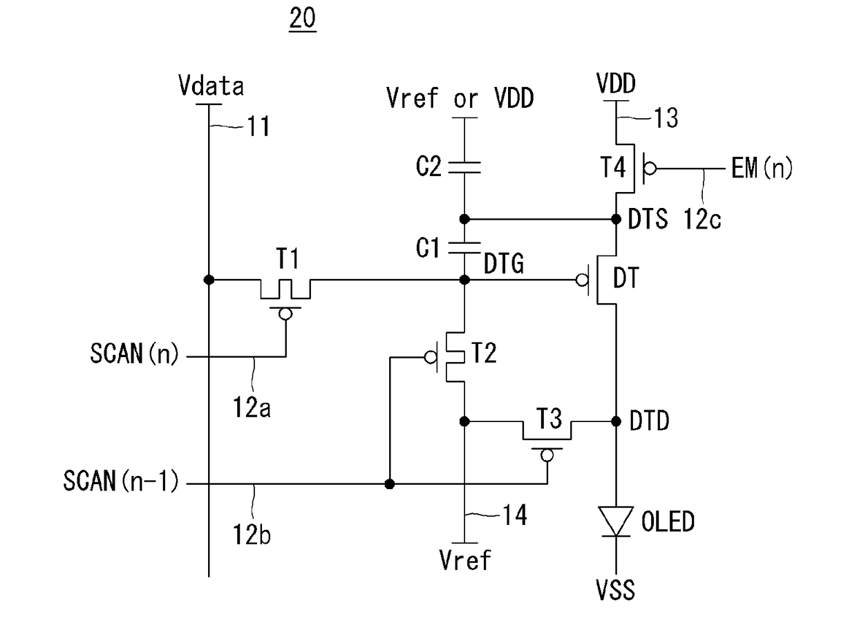
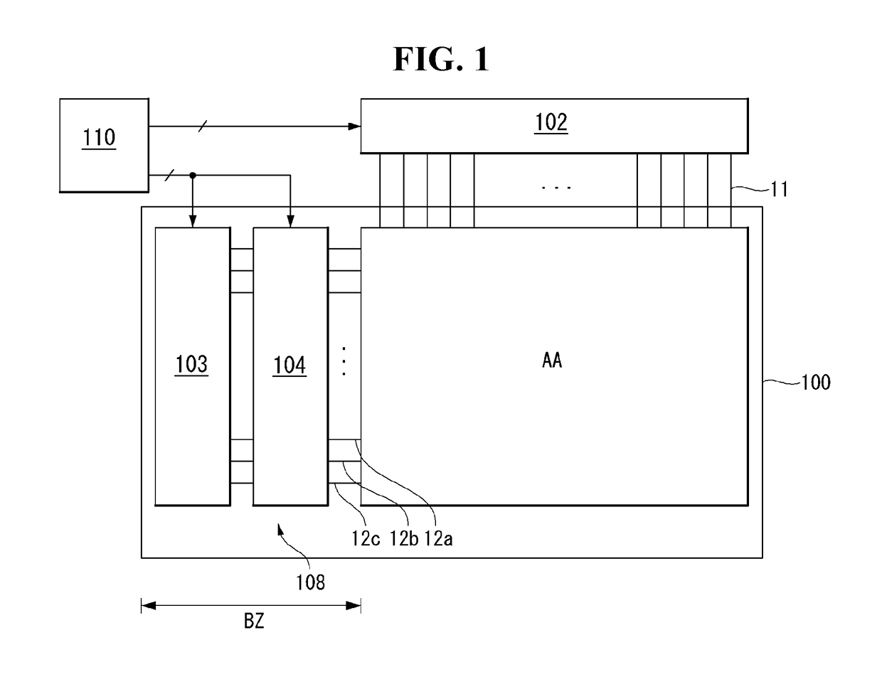
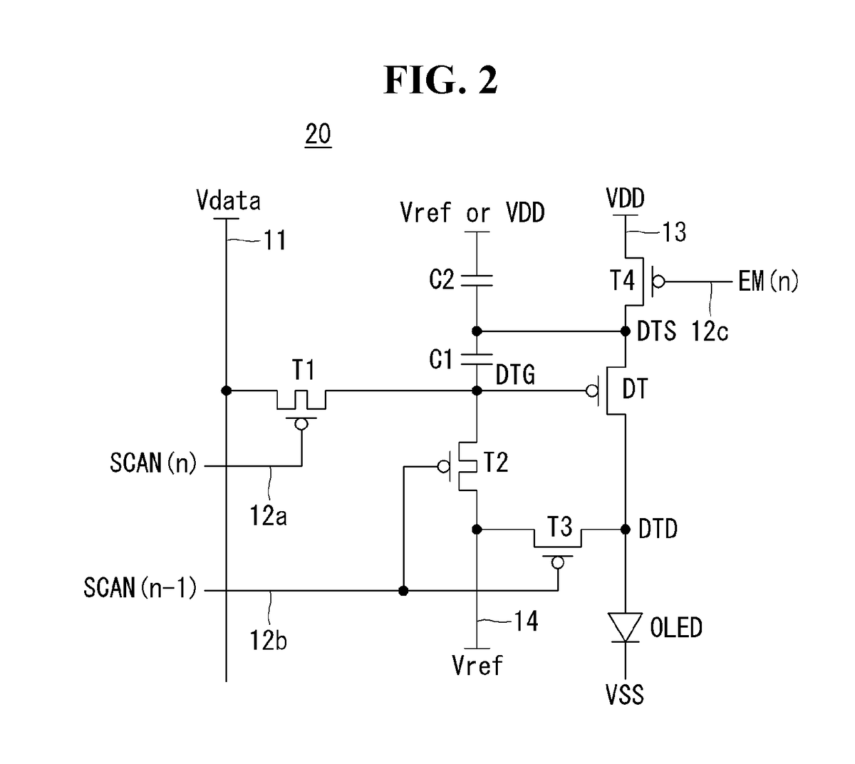
[0035]Reference will now be made in detail to embodiments of the present disclosure, examples of which are illustrated in the accompanying drawings. However, the present disclosure is not limited to embodiments disclosed below, and may be implemented in various forms. These embodiments are provided so that the present disclosure will be exhaustively and completely described, and will fully convey the scope of the present disclosure to those skilled in the art to which the present disclosure pertains. The present disclosure is only defined by the scope of the claims.

[0036]Shapes, sizes, ratios, angles, number, and the like illustrated in the drawings for describing embodiments of the present disclosure are merely exemplary, and the present disclosure is not limited thereto. Like reference numerals designate like elements throughout. In the following description, when a detailed description of well-known functions or configurations related to this document is determined to unnecessari...


PUM


Abstract

An electroluminescent display is disclosed. An electroluminescent display comprises a display panel including a plurality of pixels, each of the plurality of pixels including subpixels. A pixel circuit of each subpixels includes a driving transistor configured to drive the electroluminescent diode, a first switching transistor configured to supply a first voltage to a gate of the driving transistor in response to a first scan signal, a second switching transistor configured to supply a second voltage to the gate of the driving transistor in response to a second scan signal, a third switching transistor configured to supply the second voltage to a first electrode of the driving transistor in response to the second scan signal, a fourth switching transistor configured to supply a first supply voltage to a second electrode of the driving transistor in response to an emission control signal, a first capacitor between a first node connected to the gate electrode of the driving transistor and a second node connected to the second electrode of the driving transistor, and a second capacitor between the second node and a power supply line supplied with the second voltage or the first supply voltage.

Description

[0001]This application claims the benefit of Korean Patent Application No. 10-2016-0183098 filed on Dec. 29, 2016, and Korean Patent Application No. 10-2017-0016125 filed on Feb. 6, 2017, each of which is incorporated herein by reference in its entirety.BACKGROUNDTechnical Field[0002]The present disclosure relates to an electroluminescent display.Discussion of the Related Art[0003]An electroluminescent display is classified into an inorganic electroluminescent display and an organic electroluminescent display depending on a material of an emission layer. An active matrix organic light emitting diode (OLED) display includes a plurality of OLEDs capable of emitting light by themselves and has many advantages, such as fast response time, high emission efficiency, high luminance, wide viewing angle, and the like.[0004]An OLED serving as a self-emitting element includes an anode, a cathode, and an organic compound layer between the anode and the cathode. The organic compound layer typica...

Claims


Application Information

Patent Timeline
IPC IPC(8): G09G3/3258H01L27/32
CPCG09G3/3258G09G2300/0819H01L27/3265H01L27/3262G09G3/3208G09G3/3233G09G2300/0814G09G2300/0852G09G2300/0866G09G2320/0233G09G2320/0238G09G2320/0252G09G2320/045H10K59/1213H10K59/1216
Inventor CHANG, SUNGWOOKYOO, JUHNSUKKIM, JUNGCHULYOON, SUNGWOOKKO, HOYOUNG
Owner LG DISPLAY CO LTD
Why Eureka
Try Eureka