Method for fabricating semiconductor device

Active Publication Date: 2018-07-05
MITSUBISHI ELECTRIC CORP
View PDF2 Cites 0 Cited by
  • Summary
  • Abstract
  • Description
  • Claims
  • Application Information

AI Technical Summary

Benefits of technology

The present invention provides a fabrication method for a semiconductor device that addresses the problem of uneven surfaces caused by the opening portion in the silicon oxide film. The method involves extending a structural member that is less prone to etching by hydrofluoric acid than the silicon oxide film, into the opening portion. This blocking action prevents the progress of hydrofluoric acid and prevents the structural member from separating from the silicon oxide film. The technical effect of this method is the suppression of uneven surfaces and the prevention of separation of the structural member from the silicon oxide film.

Problems solved by technology

For example, foreign substances on the Si surfaces may cause abnormal diffusions during addition of impurities thereto.

Method used


Image

  • Method for fabricating semiconductor device
  • Method for fabricating semiconductor device
  • Method for fabricating semiconductor device

Examples


first embodiment

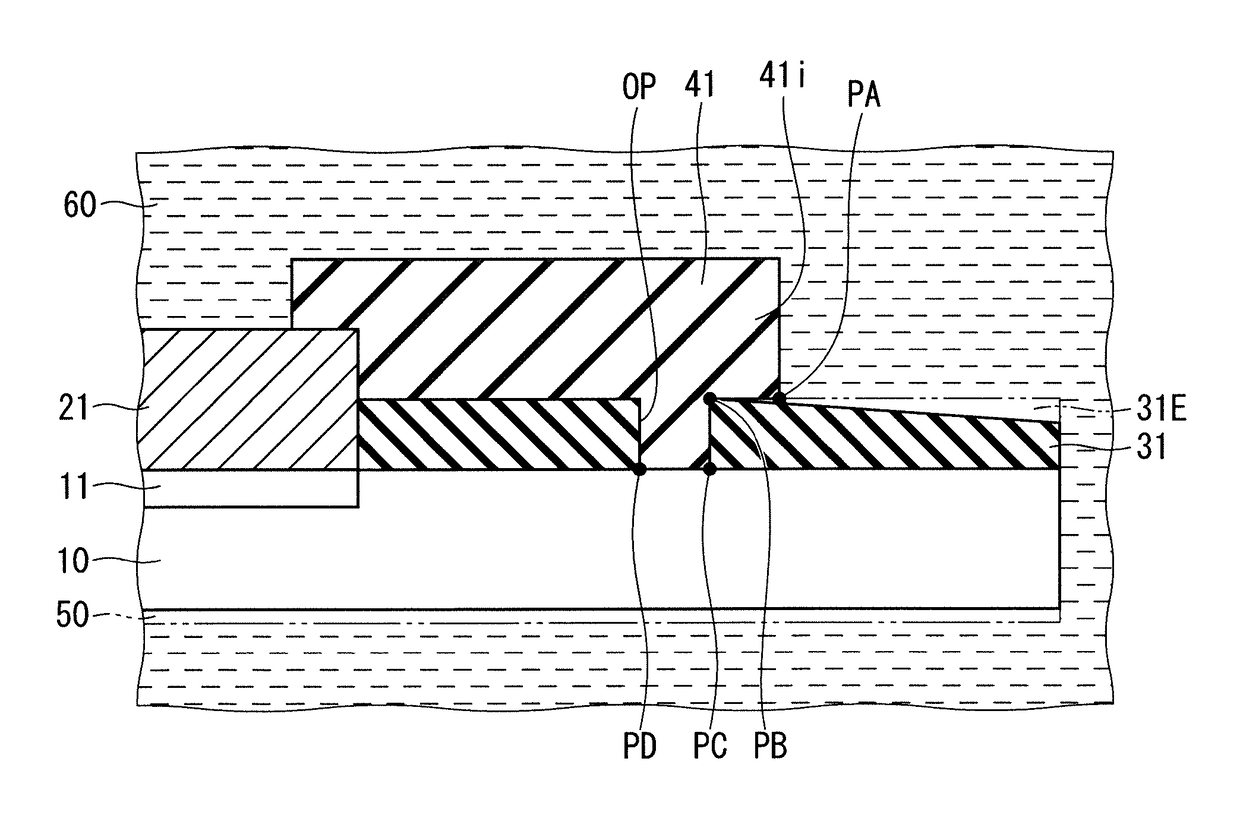
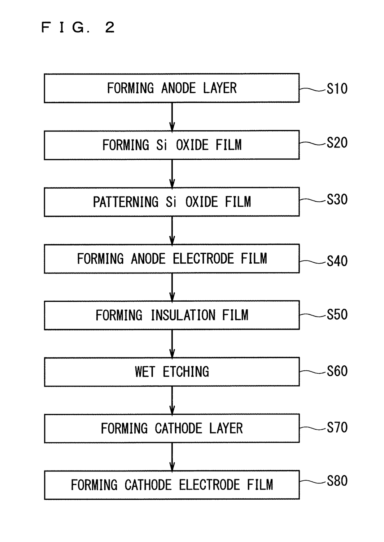
[0043]FIG. 1 is a partial cross-sectional view schematically illustrating the structure of a diode 91 (a semiconductor device) according to the present embodiment. More specifically, the diode 91 is a pin diode as an power semiconductor device. The diode 91 includes a Si substrate 10 (a silicon substrate), an anode layer 11, a cathode layer 12, an anode electrode film 21, a cathode electrode film 22, a SiO2 film 31 (a silicon oxide film), and a protective structural member 41 (a structural member).

[0044]The Si substrate 10 is a single-crystal substrate formed of Si. The anode layer 11 is a p-type impurity-diffusion layer, which is provided on a center portion (in the left side in the figure) of the upper surface (one surface) of the Si substrate 10. The cathode layer 12 is an n-type impurity-diffusion layer, which is provided on the lower surface (the other surface) of the Si substrate 10.

[0045]The anode electrode film 21 is provided on the anode layer 11. The anode electrode film 2...

second embodiment

[0057]FIG. 8 is a partial cross-sectional view schematically illustrating the structure of a diode 92 according to the present embodiment. The diode 92 includes a SiO2 film 32 (a silicon oxide film) and a protective structural member 42 (a structural member), instead of the SiO2 film 31 and the protective structural member 41 (FIG. 1: the first embodiment). In the present embodiment, the protective structural member 42 is constituted by a single insulation film 42i. The SiO2 film 32 includes two or more opening portions OP. The insulation film 42i as the protective structural member 42 is provided on the SiO2 film 32 and reaches a Si substrate 10 in the respective opening portions OP. Referring to FIG. 9 and FIG. 10, respectively, the diode 92 can be fabricated through substantially the same processes as the processes in FIGS. 3 and 4 according to the first embodiment. Further, a two-dot chain-line portion 32E (FIG. 10) in the SiO2 film 32 schematically represents the etched portion...

third embodiment

[0060]FIG. 11 is a partial cross-sectional view schematically illustrating the structure of a diode 93 according to the present embodiment. The diode 93 includes a protective structural member 43 (a structural member), instead of the protective structural member 41 (FIG. 1: the first embodiment). The protective structural member 43 includes an insulation film 43i and a metal film 43m. The metal film 43m reaches a Si substrate 10 in an opening portion OP in a SiO2 film 31. The metal film 43m preferably penetrates the opening portion OP. More preferably, the metal film 43m has a larger thick dimension than the depth dimension of the opening portion OP. Further, more preferably, the metal film 43m has a T-shaped cross-sectional shape. Thus, the metal film 43m has a portion protruded from the opening portion OP, on the SiO2 film 31.

[0061]The insulation film 43i covers the metal film 43m. The insulation film 43i is disposed on the SiO2 film 31 on which the metal film 43m is provided and,...


PUM


Abstract

A silicon oxide film having at least one opening portion is formed, on a silicon substrate. A structural member formed of a material less prone to be etched by hydrofluoric acid than a silicon oxide film is formed, wherein the structural member is provided on the silicon oxide film and reaches the silicon substrate in the opening portion. Wet etching using hydrofluoric acid is performed, on the silicon substrate on which the silicon oxide film and the structural member are provided. The interface between the silicon oxide film and the structural member is exposed to hydrofluoric acid, in performing the wet etching.

Description

TECHNICAL FIELD[0001]The present invention relates to methods for fabricating semiconductor devices and, more particularly, relates to methods for fabricating semiconductor devices using wet etching.BACKGROUND ART[0002]In methods for fabricating semiconductor devices, it is necessary to clean the surfaces of Si (silicon) substrates, in some cases. More specifically, in some cases, it is necessary to remove natural oxide films or foreign substances from the surfaces of Si substrates. For example, foreign substances on the Si surfaces may cause abnormal diffusions during addition of impurities thereto.[0003]For example, according to Japanese Patent Application Laid-Open No. 8-339996 (1996) (Patent Document 1), a SiO2 film (a silicon oxide film) is formed on a Si substrate. Further, a SiOx film (x>2) is formed on the silicon oxide film. Further, an opening portion is formed in the layer-laminated structure constituted by the silicon oxide film and the SiOx film. Along with the proce...

Claims


Application Information

Patent Timeline
IPC IPC(8): H01L21/56H01L29/868H01L21/306
CPCH01L21/56H01L29/868H01L21/30604H01L29/6609H01L29/0619H01L21/31111H01L23/3171H01L21/0206
Inventor KACHI, TAKAOYOSHIURA, YASUHIRO
Owner MITSUBISHI ELECTRIC CORP
Why Eureka
Try Eureka