Semiconductor integrated circuit device

a technology of integrated circuit device and semiconductor, which is applied in the direction of semiconductor device, semiconductor/solid-state device details, electrical apparatus, etc., can solve the problems of increase in cost and decrease in and achieve the effect of reducing design margin, and improving the performance of semiconductor integrated circuit devi

Active Publication Date: 2018-07-05
SOCIONEXT INC
View PDF7 Cites 7 Cited by
  • Summary
  • Abstract
  • Description
  • Claims
  • Application Information

AI Technical Summary

Benefits of technology

[0008]In view of the foregoing background, it is therefore an object of the present disclosure to reduce, in a semiconductor integrated circuit device including a standard cell with a fin transistor, such an influence of a cell arrangement on the characteristics of the fin transistor and eventually improve the performance of the semiconductor integrated circuit device.
[0010]According to this aspect of the present disclosure, the distance between the active fin and the fin located closer to the end of the cell than the active fin is, i.e., the dummy fin, is determined uniquely regardless of the configuration of another standard cell arranged adjacent to the first standard cell. Thus, the active transistor formed by the active fin has a constant current characteristic regardless of the cell arrangement. This allows for reducing a design margin, and eventually improving the performance of the semiconductor integrated circuit device.
[0012]According to this aspect of the present disclosure, in the first and second standard cells, the distance between an active fin located near the cell boundary and a dummy fin disposed on the cell boundary is determined uniquely regardless of the configuration of an adjacent standard cell. Thus, the active transistor arranged near the cell boundary has a constant current characteristic regardless of the cell arrangement. This allows for reducing a design margin, and eventually improving the performance of the semiconductor integrated circuit device. Furthermore, the first and second standard cells share the dummy fin. This allows for reducing the cell area while achieving the above advantage. Consequently, the overall circuit area and manufacturing cost of the semiconductor integrated circuit device may be cut down.
[0014]According to this aspect of the present disclosure, the fin located closest to the cell row boundary in the first standard cell and the dummy fin in the second standard cell are disposed at the same position in the second direction. Thus, the distance between the active fin of the second cell row, located near the cell row boundary, and the fin of the first cell row, located opposite the active fin across the cell row boundary, is determined uniquely regardless of the configuration of the standard cell in the first cell row. Thus, the active transistor located near the cell row boundary has a constant current characteristic regardless of the cell arrangement. This allows for reducing a design margin, and eventually improving the performance of the semiconductor integrated circuit device.
[0015]The present disclosure allows for reducing, in a semiconductor integrated circuit device including a standard cell with a fin transistor, an influence of a cell arrangement on the characteristics of the fin transistor. This thus allows for improving the performance of the semiconductor integrated circuit device.

Problems solved by technology

This, however, may cause a decrease in the performance of the semiconductor integrated circuit or an increase in cost, which is not beneficial.

Method used


Image

  • Semiconductor integrated circuit device
  • Semiconductor integrated circuit device
  • Semiconductor integrated circuit device

Examples


first embodiment

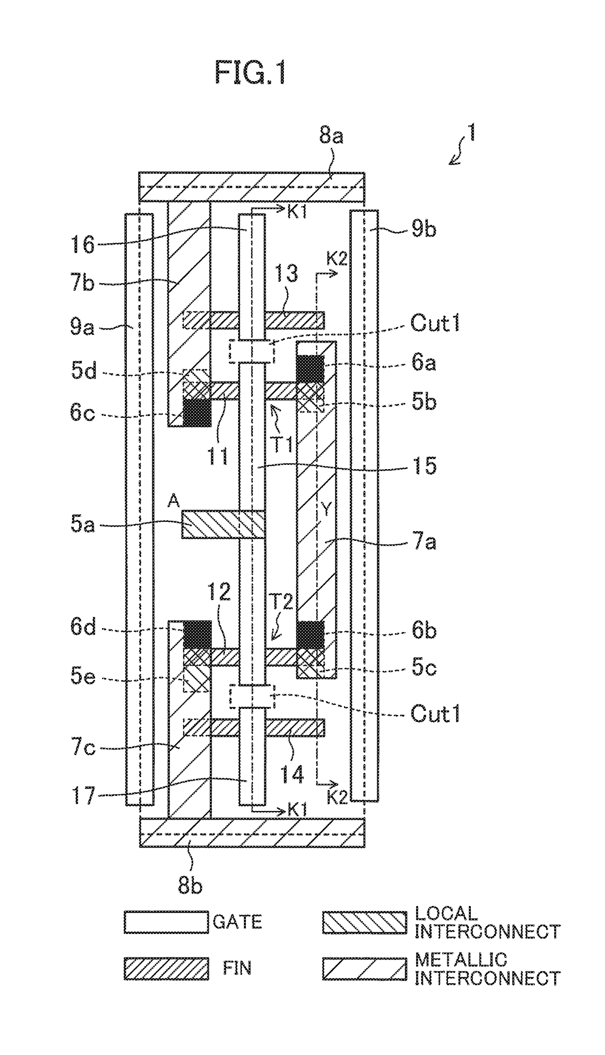
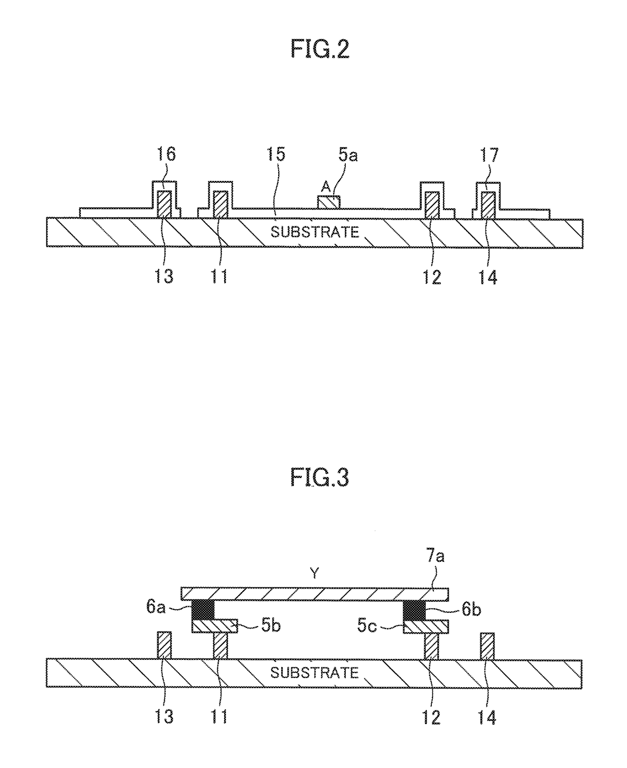
[0032]FIG. 1 is a plan view illustrating an exemplary layout design for a standard cell included in a semiconductor integrated circuit device according to a first embodiment. FIG. 2 is a cross-sectional view taken along the plane K1-K1 in the layout design of FIG. 1, and FIG. 3 is a cross-sectional view taken along the plane K2-K2 in the layout design of FIG. 1. In this embodiment, an inverter cell will be described for the sake of simplicity, but the present disclosure is not limited thereto.

[0033]The standard cell 1 illustrated in FIGS. 1-3 includes a fin transistor. The standard cell 1 includes a plurality of fins 11, 12, 13, and 14 extending in the lateral direction on the paper (corresponding to a first direction), and arranged in the vertical direction on the paper (corresponding to a second direction perpendicular to the first direction). In FIG. 1 and other plan views, a fin transistor is comprised of a fin and a gate formed on the fin. A local interconnect is formed so as t...

second embodiment

[0041]FIG. 6 is a plan view illustrating an exemplary layout design for a semiconductor integrated circuit device according to a second embodiment. In the following description of the second embodiment, an inverter cell will be described as one example for the sake of simplicity. However, this is only an exemplary embodiment of the present disclosure. Adjoining standard cells 2A and 2B may be cells of mutually different types.

[0042]The standard cells 2A and 2B illustrated in FIG. 6 each include a fin transistor. The standard cell 2A includes a plurality of fins 21 and 22 extending in the lateral direction on the paper (corresponding to a first direction), and arranged in the vertical direction on the paper (corresponding to a second direction perpendicular to the first direction). The fins 21 and 22 are active fins, and form part of active transistors which contribute to the logical function of the standard cell 2A. A gate line 26 is provided on the fins 21 and 22. Likewise, the sta...

third embodiment

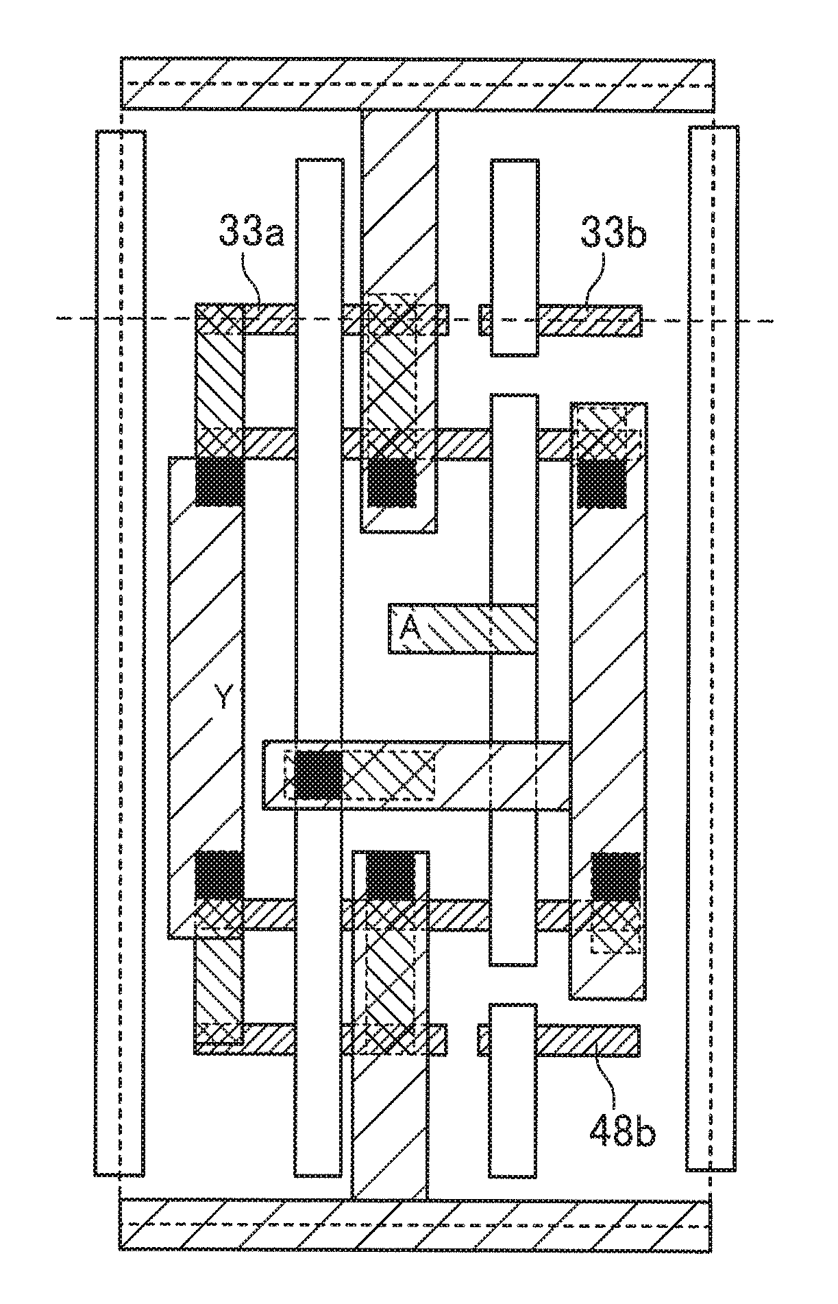
[0050]FIG. 10 is a plan view illustrating an exemplary layout design for a semiconductor integrated circuit device according to a third embodiment. FIG. 10 illustrates a first cell row CR1 including standard cells 3A, 3B, 3C, and 3D that are arranged side by side in the lateral direction on the paper (corresponding to a first direction), and a second cell row CR2 including standard cells 3E, 3F, 3G, and 3H that are arranged side by side in the lateral direction on the paper, and disposed adjacent to the first cell row CR1 in the vertical direction on the paper (corresponding to a second direction perpendicular to the first direction). FIG. 10 illustrates only cell frames and fins arranged along the cell row boundary CRB between the first and second cell rows CR1 and CR2 for the sake of simplicity with illustration of the other fins omitted. In the first cell row CR1, fins 31, 32, 33a, 33b, and 34 extending in the lateral direction on the paper are arranged in a straight line along t...


PUM


Abstract

Disclosed herein is a semiconductor integrated circuit device which includes a standard cell with a plurality of fins extending in a first direction and arranged in a second direction that is perpendicular to the first direction. An active fin of the fins forms part of an active transistor. A dummy fin of the fins is disposed between the active fin and an end of the standard cell.

Description

CROSS-REFERENCE TO RELATED APPLICATIONS[0001]This continuation of U.S. patent application Ser. No. 15 / 052,521 filed on Feb. 24, 2016, which is a continuation of International Application No. PCT / JP2014 / 002236 filed on Apr. 21, 2014, which claims priority to Japanese Patent Application No. 2013-177182 filed on Aug. 28, 2013. The entire disclosures of these applications are hereby incorporated by reference.BACKGROUND[0002]The present disclosure relates to a semiconductor integrated circuit device including a standard cell with a transistor having a fin structure.[0003]A standard cell design has been known as a method of forming a semiconductor integrated circuit on a semiconductor substrate. The standard cell design refers to a method of designing a large-scale integrated circuit (LSI) chip by providing in advance, as standard cells, unit logic elements having particular logic functions (for example, an inverter, a latch, a flip-flop, and a full adder), laying out those standard cells...

Claims


Application Information

Patent Timeline
Patent Type & Authority Applications(United States)
IPC IPC(8): H01L27/02H01L23/528H01L29/66H01L21/8238H01L27/088H01L27/092H01L27/12
CPCH01L27/0924H01L27/1211H01L27/0207H01L23/528H01L27/0886H01L2924/0002H01L21/823821H01L29/6681H01L2924/00
Inventor SHIMBO, HIROYUKI
Owner SOCIONEXT INC
Why Eureka
Try Eureka