High-frequency module

a high-frequency module and module technology, applied in the direction of printed circuit manufacturing, cross-talk/noise/interference reduction, printed circuit aspects, etc., can solve the problem of wiring substrate cracking or warping

Active Publication Date: 2018-07-19
MURATA MFG CO LTD
View PDF5 Cites 5 Cited by
  • Summary
  • Abstract
  • Description
  • Claims
  • Application Information

AI Technical Summary

Benefits of technology

[0016]Furthermore, the high-frequency module may further include: a shield film that covers a surface of the sealing resin layer except for the island-shaped region. In this case, a component that is not to be shielded from electromagnetic waves can be arranged in the part corresponding to the island-shaped region. In addition, electromagnetic waves from the top surface of the island-shaped region can be prevented from affecting a component mounted in a region other than the island-shaped region.
[0017]The high-frequency module may further include: a ground electrode that is arranged inside the wiring substrate and outside the island-shaped region; and a via that connects the shield wall and the ground electrode to each other. In this case, the shield film, the shield wall, and the ground electrode are arranged so as to surround a component in a region other than the island-shaped region, and therefore the shielding performance between a component mounted in the island-shaped region and a component mounted in the region other than the island-shaped region can be improved.
[0018]In addition, the high-frequency module may further include: a surface layer conductor that is arranged on the main surface of the wiring substrate so as to contact each shield wall element body. In this case, since the surface area of the surface layer conductor on the main surface is increased, the heat from a laser that is used when forming grooves is more easily released. In addition, it is possible to use a common via conductor.

Problems solved by technology

However, the slit S disclosed in Patent Document 1 is formed using a method in which a groove is formed in the molding resin layer 103 and then the groove is filled with a conductive paste, and since the molding resin layer 103 is divided by this groove, there is a problem in that the wiring substrate may crack or warp due to the heat or stress generated when the high-frequency module is used.

Method used


Image

  • High-frequency module
  • High-frequency module
  • High-frequency module

Examples


first embodiment

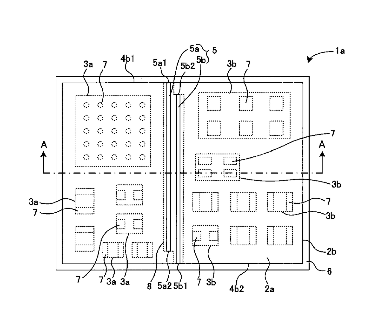
[0031]A high-frequency module la according to a first embodiment of the present disclosure will be described while referring to FIGS. 1A, 1B and 1C. FIG. 1A is a plan view of the high-frequency module 1a, FIG. 1B is a sectional view taken along A-A in FIG. 1A and looking in the direction of the arrows, and FIG. 1C is a plan view of a sealing resin layer 4. In addition, a top surface part of a shield film 6 is not illustrated in FIGS. 1A, 1B and 1C.

[0032]As illustrated in FIGS. 1A, 1B and 1C, the high-frequency module 1a according to this embodiment includes a wiring substrate 2, a plurality of components 3a and 3b that are mounted on an upper surface 2a (corresponding to “a main surface of the wiring substrate” of the present disclosure) of the wiring substrate 2, a sealing resin layer 4 that is stacked on the upper surface 2a of the wiring substrate 2, a shield film 6 that covers a surface of the sealing resin layer 4, and a shield wall 5 that is provided in the sealing resin layer...

second embodiment

[0059]A high-frequency module 1d according to a second embodiment of the present disclosure will be described while referring to FIGS. 4A and 4B. FIG. 4A is a plan view of the high-frequency module 1d, and FIG. 4B is a sectional view taken along B-B in FIG. 4A and looking in the direction of the arrows. In addition, a top surface part of the shield film 6 is not illustrated in FIG. 4A.

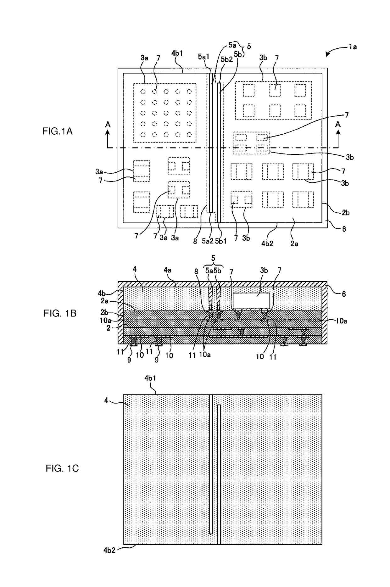
[0060]The high-frequency module 1d according to this embodiment differs from the high-frequency module la of the first embodiment described while referring to FIGS. 1A, 1B and 1C in that the area of the upper surface 2a of the wiring substrate 2 is partitioned into one central island-shaped region 2a1 and a remaining region 2a2 by a shield wall element body 51 that is substantially U-shaped in a plan view and a shield wall element body 52 that is substantially L-shaped in a plan view. The rest of the configuration is the same as that of the high-frequency module 1a of the first embodiment and therefore...

third embodiment

[0070]A high-frequency module 1g according to a third embodiment of the present disclosure will be described while referring to FIG. 8. FIG. 8 is a plan view of the high-frequency module 1g, and is a diagram corresponding to each of FIGS. 4A and 4B.

[0071]The high-frequency module 1g according to this embodiment differs from the high-frequency module 1e of the modification of the second embodiment described while referring to FIG. 6 in that, as illustrated in FIG. 8, the upper surface 4a and the peripheral side surfaces 4b of the sealing resin layer 4 and the side surfaces 2b of the wiring substrate 2 are covered by a shield film 61 having an opening 12 in a part thereof that is superposed in a plan view with the island-shaped region 2a3. The rest of the configuration is the same as that of the high-frequency module 1e, and therefore the same symbols are used and the description thereof is omitted.

[0072]Furthermore, as illustrated in FIG. 9, a ground electrode 10a1 that is arranged o...


PUM


Abstract

A high-frequency module la includes: a wiring substrate 2; a plurality of components 3a and 3b that are mounted on an upper surface 2a of the wiring substrate 2; a sealing resin layer 4 that is stacked on the upper surface 2a of the wiring substrate 2; a shield film 6 that covers a surface of the sealing resin layer 4; and a shield wall 5 that is provided in the sealing resin layer 4. The shield wall 5 is formed of two shield wall element bodies 5a and 5b that have straight line shapes in a plan view, and the two shield wall element bodies 5a and 5b are arranged such that the shield wall element bodies each have one end surface that is not exposed at a different peripheral side surface 4b of the sealing resin layer 4.

Description

[0001]This is a continuation of International Application No. PCT / JP2016 / 076753 filed on Sep. 12, 2016 which claims priority from Japanese Patent Application No. 2015-180971 filed on Sep. 14, 2015. The contents of these applications are incorporated herein by reference in their entireties.BACKGROUND OF THE DISCLOSUREField of the Disclosure[0002]The present disclosure relates to a high-frequency module that includes a sealing resin layer that covers a plurality of components mounted on a wiring substrate, and a shield layer that is for preventing the electromagnetic wave interference between the components.Description of the Related Art[0003]A shield layer is provided in a high-frequency module installed in a mobile terminal device or the like in order to block electromagnetic waves. Among high-frequency modules of this type, there are high-frequency modules in which components mounted on a wiring substrate are covered by a molding resin and a shield layer is provided so as to cover ...

Claims


Application Information

Patent Timeline
Patent Type & Authority Applications(United States)
IPC IPC(8): H01L23/31H01L25/04H01L25/18H01L23/00H05K9/00
CPCH01L23/3121H01L25/04H01L25/18H01L24/82H05K9/0081H01L2924/181H01L2924/09701H01L2924/3025H01L23/16H01L23/552H01L24/16H01L25/0655H01L25/16H01L2224/16225H01L2924/00014H01L2924/10253H01L2924/10329H01L2924/15192H01L2924/15313H01L2924/19041H01L2924/19042H01L2924/19043H01L2924/19105H01L2924/3511H05K1/0216H05K1/0243H05K1/0298H05K1/181H05K3/284H05K9/0022H05K9/0084H05K2201/09972H05K2203/1322H01L2924/00012H01L2224/13099H01L23/28
Inventor OTSUBO, YOSHIHITO
Owner MURATA MFG CO LTD
Why Eureka
Try Eureka