Thin fan-out multi-chip stacked package structure and manufacturing method thereof

a technology of multi-chip stack and package structure, which is applied in the direction of semiconductor devices, semiconductor/solid-state device details, electrical devices, etc., can solve the problems of easy short-circuit caused by wire sweep, the total thickness of the multi-chip stack package structure cannot be reduced, etc., and achieve the effect of increasing the yield of the package and enhancing the manufacturing precision

Active Publication Date: 2018-07-26
POWERTECH TECHNOLOGY
View PDF0 Cites 13 Cited by
  • Summary
  • Abstract
  • Description
  • Claims
  • Application Information

AI Technical Summary

Benefits of technology

[0007]Through the above technical means, the disclosure is able achieve the application of an ultra-thin fan-out wafer-level package process in which the substrate thickness is neglected. The overall package thickness is very close to the chip stack height and may be in a range not exceeding 100 micrometers. Moreover, the disclosure may also be applied in a panel-level package process. The disclosure may further be incorporated as a ball-grid array (BGA) package type. The stacking, wiring, and encapsulating of the chips are introduced in the wafer-level or panel-level packaging process before the redistribution layer is formed to render an ultra-thin package structure. Therefore, other than the differences in the carrier and the formation of the redistribution layer, the chip disposition, wiring bonding, and encapsulation step may all adopt existing packaging techniques. Furthermore, with the aid of the alignment structure, the manufacturing precision may be further enhanced, thereby increasing the yield of the package.

Problems solved by technology

However, the multi-chip stack package structure formed by this method would at least require the thickness of the substrate and the height of the wiring arc.
In other words, the total thickness of the multi-chip stack package structure cannot be reduced.
In particular, in situations requiring long bonding wires, issues such as short-circuit caused by wire sweep may occur easily during the step of forming an encapsulant.

Method used


Image

  • Thin fan-out multi-chip stacked package structure and manufacturing method thereof
  • Thin fan-out multi-chip stacked package structure and manufacturing method thereof
  • Thin fan-out multi-chip stacked package structure and manufacturing method thereof

Examples


Embodiment Construction

[0017]In the following, embodiments of the disclosure are described in detail with reference to figures. However, it should be mentioned that, the figures are all simplified schematics showing the basic structure or implementation of the disclosure in an illustrative manner. Therefore, only components and combinations pertinent to the present application are shown, and the components shown in the figures are not drawn to scale in terms of the number, shape, and size of actual implementation. Certain size ratios and other relating size ratios are exaggerated or simplified to provide a clearer description. The number, shape, and size ratio of actual implementation are open designs, and the detailed component layout may be more complicated.

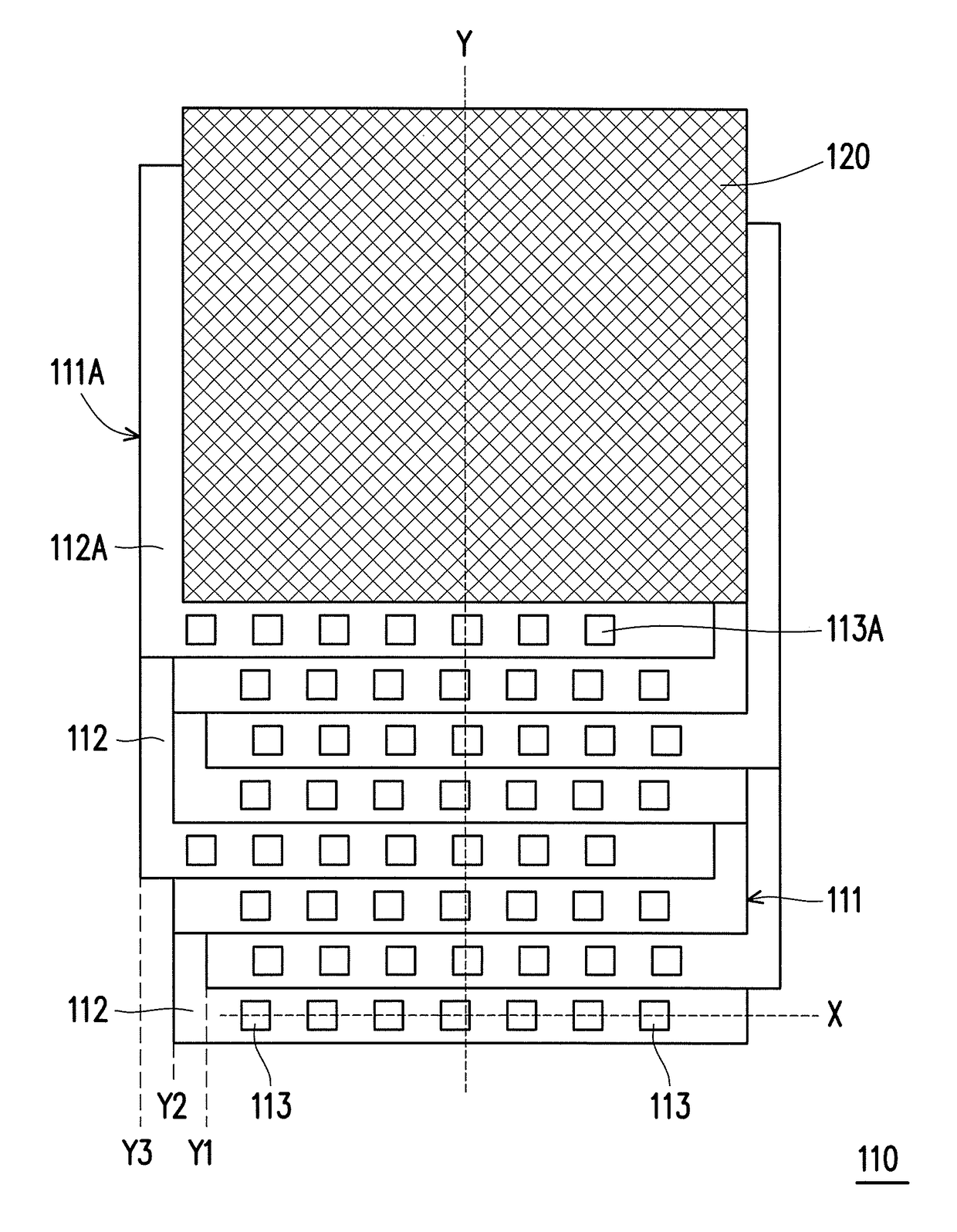
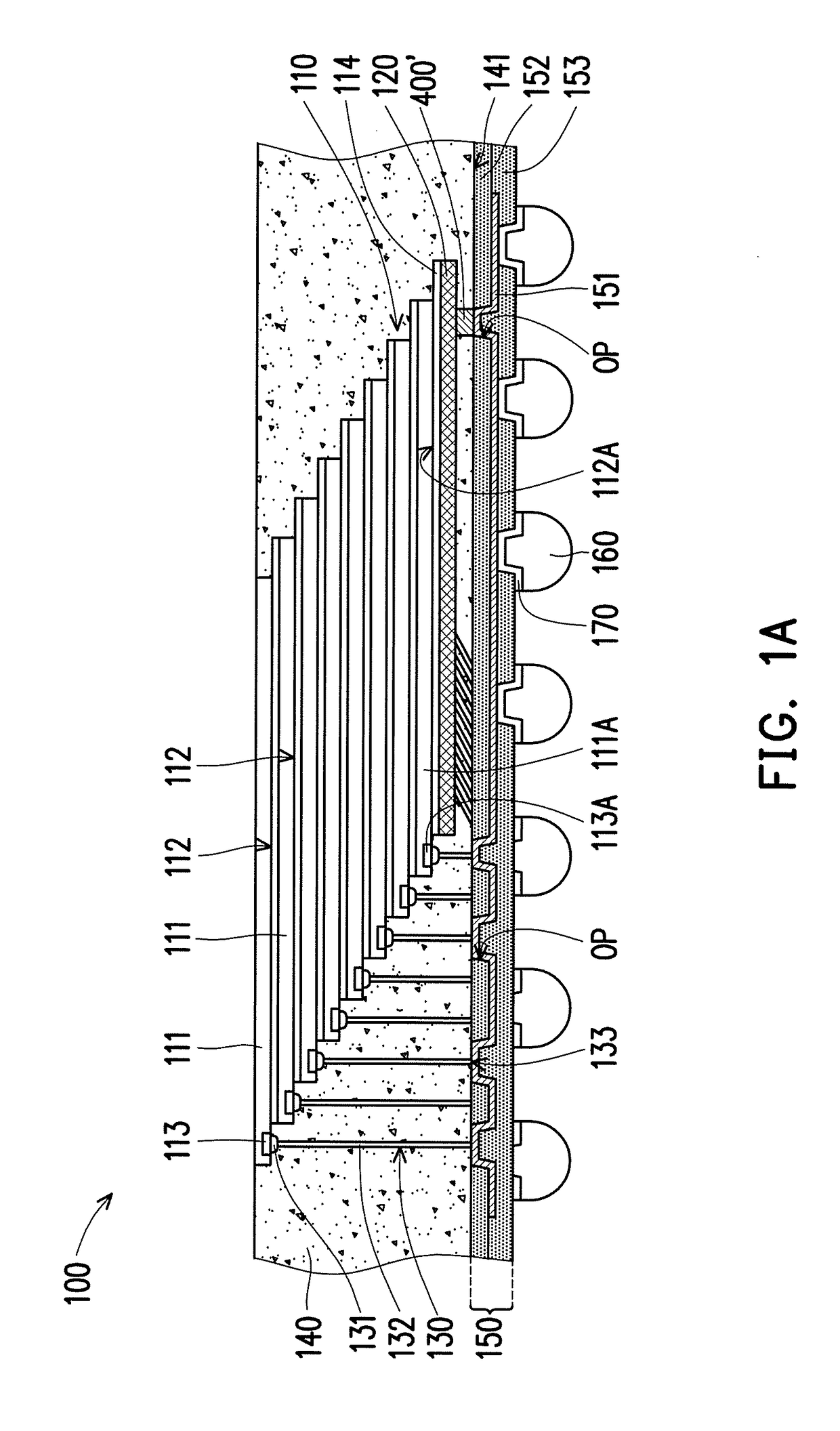
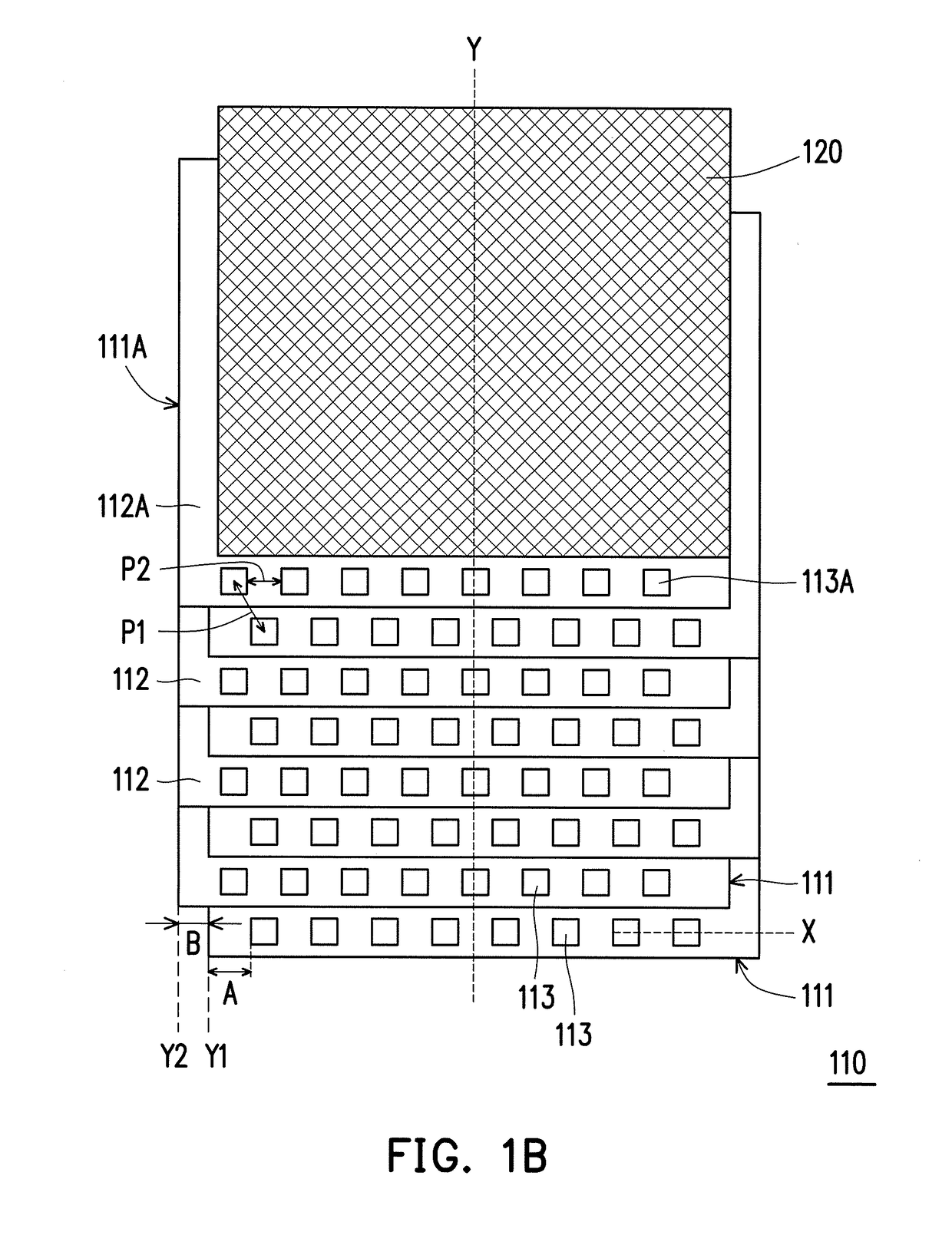
[0018]According to a first embodiment of the disclosure, FIG. 1A illustrates a cross-sectional view of a thin fan-out multi-chip stacked package structure 100. FIG. 1B illustrates a schematic top view of a chip stack 110 in the thin fan-out multi-chi...


PUM


Abstract

A thin fan-out multi-chip stacked package structure including a plurality of stacked chips is provided. The electrodes of the stacked chips and the active surface of the top chip are exposed. A dummy spacer and an alignment structure are disposed over the active surface. Each bonding wire has a bonding thread bonded to a chip electrode and an integrally-connected vertical wire segment. A flat encapsulant encapsulates the chip stacked structure and the bonding wires. Polished cross-sectional surfaces of the bonding wires and a surface of the alignment structure are exposed by the flat surface of the encapsulant. A redistribution layer structure is formed on the flat surface. A passivation layer covers the flat surface and exposes the polished cross-sectional surfaces and the alignment structure. Fan-out circuits are formed on the passivation layer and are connected to the polished cross-sectional surfaces of the bonding wires and the alignment structure.

Description

CROSS-REFERENCE TO RELATED APPLICATION[0001]This application claims the priority benefit of Taiwan application serial no. 106102928, filed on Jan. 25, 2017. The entirety of the above-mentioned patent application is hereby incorporated by reference herein and made a part of this specification.BACKGROUND OF THE INVENTIONField of the Invention[0002]The disclosure relates to the field of semiconductor chip packaging, and more particularly, to a thin fan-out multi-chip stacked package structure and a manufacturing method thereof.Description of Related Art[0003]In the known multi-chip stack package structure, a plurality of semiconductor chips are stacked upward on a substrate one by one. The active surfaces of the chips face upward and the complete bonding wires formed by wiring bonding electrically connect the chips to the substrate. In general, the bonding threads of the bonding wires are bonded to bonding pads of the chips, the wire ends of the bonding wires are bonded to contact fing...

Claims


Application Information

Patent Timeline
Patent Type & Authority Applications(United States)
IPC IPC(8): H01L23/00H01L23/31H01L23/544
CPCH01L24/96H01L2924/181H01L23/544H01L23/3171H01L23/3128H01L21/568H01L23/16H01L2223/54426H01L2223/54486H01L2224/214H01L24/19H01L24/20H01L2224/04105H01L2224/12105H01L2224/32145H01L2224/32225H01L2224/32245H01L2224/33181H01L2224/73217H01L2224/73267H01L2224/92244H01L2924/18162H01L2924/3511
Inventor CHANG, CHIA-WEICHUANG, YONG-CHENGLIN, YU-TSO
Owner POWERTECH TECHNOLOGY
Why Eureka
Try Eureka