Coplanar double gate electrode oxide thin film transistor and manufacture method thereof

a technology of oxide thin film transistor and double gate electrode, which is applied in the field of display technology, to achieve the effects of reducing the diffusion of igzo internal defects, effective reducing light affecting stability, and improving the electrical stability of thin film transistor

Active Publication Date: 2018-07-26
WUHAN CHINA STAR OPTOELECTRONICS TECH CO LTD
View PDF2 Cites 3 Cited by
  • Summary
  • Abstract
  • Description
  • Claims
  • Application Information

AI Technical Summary

Benefits of technology

[0053]First, the thin film transistor of the present disclosure is designed as a double gate electrode structure, wherein the bottom electrode and the top electrode may as the light blocking layer, effectively reducing the light affect the stability of the oxide film transistor (particularly the thin film transistor using the amorphous IGZO thin film as the oxide semiconductor layer). Otherwise, the bottom gate electrode has the opposite electric field to the top gate electrode, this can reduce the diffusion of the IGZO internal defects into the channel and also improve the electrical stability of the thin film transistor using the amorphous IGZO thin film as the oxide semiconductor layer, such as the voltage bias test and the current bias test.
[0054]Second, the source contact area, the drain contact area and the oxide semiconductor layer of the present disclosure are coplanar structure, rather than having the step difference structure, so that the portion of the source electrode contact area and the drain electrode contact area respectively overlapped between the gate electrode is less, can reduce the intrinsic capacitance of the thin film transistor, thereby reducing the RC delay and improve the response speed of thin film transistor.
[0055]Finally, the bottom gate electrode and the substrate are designed in a coplanar structure so that the first gate insulating layer and the second gate insulating layer are both flat and there is no problem of step coverage. Compared with the planar gate insulating layer, the gate insulating layer having a stepped structure is easily punctured with the insulating layer film at the step edge thereof, and it is generally necessary to increase the thickness of the gate insulating layer having the step structure in order to avoid the breakdown problem. In the present disclosure, since the gate insulating layer is planar and there is no breakdown problem at the step edge, the gate insulating layer can be designed to be relatively thin, thereby lowering the driving voltage and reducing the power consumption.

Problems solved by technology

However, there is an important constraint on the technology used in mass production of display panels—the stability is not sufficient, therefore, it is necessary to conduct in-depth study of the technology, improve and optimize the existing oxide thin film transistor structure, it has a more stable device performance.

Method used


Image

  • Coplanar double gate electrode oxide thin film transistor and manufacture method thereof
  • Coplanar double gate electrode oxide thin film transistor and manufacture method thereof
  • Coplanar double gate electrode oxide thin film transistor and manufacture method thereof

Examples


embodiment 1

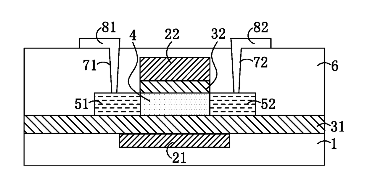
[0058]The present embodiment provides a coplanar double gate electrode oxide thin film transistor, as shown in FIG. 1, includes the following structure:

[0059]a substrate 1 at the bottom, the substrate 1 is provided with a groove which is recessed toward the inside of the substrate;

[0060]a patterned bottom gate electrode 21 formed in the groove of the substrate 1, and the upper surface of the bottom electrode 21 and the upper surface of the substrate 1 are in the same horizontal plane, so that the bottom gate electrode 21 and the substrate 1 form a coplanar structure;

[0061]a first gate electrode insulating layer 31 formed on the substrate 1 and the bottom electrode 21, the first gate electrode insulating layer is made of the SiOx or the aluminum oxide thin film as the insulating layer of the bottom gate electrode, due to the bottom gate electrode and the substrate are coplanar structure, the first gate electrode insulating layer has the planar structure, rather than the staircase str...

embodiment 2

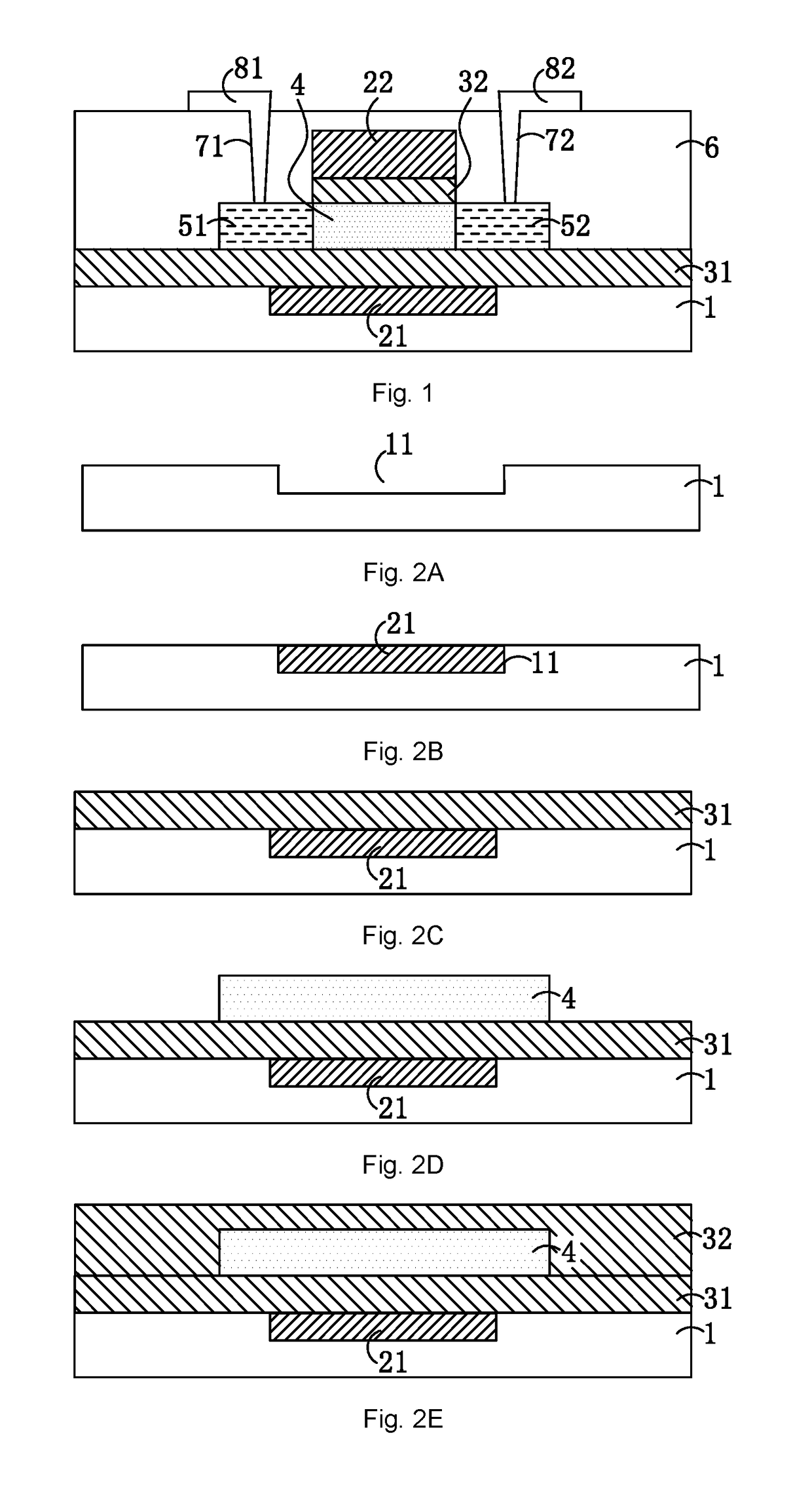
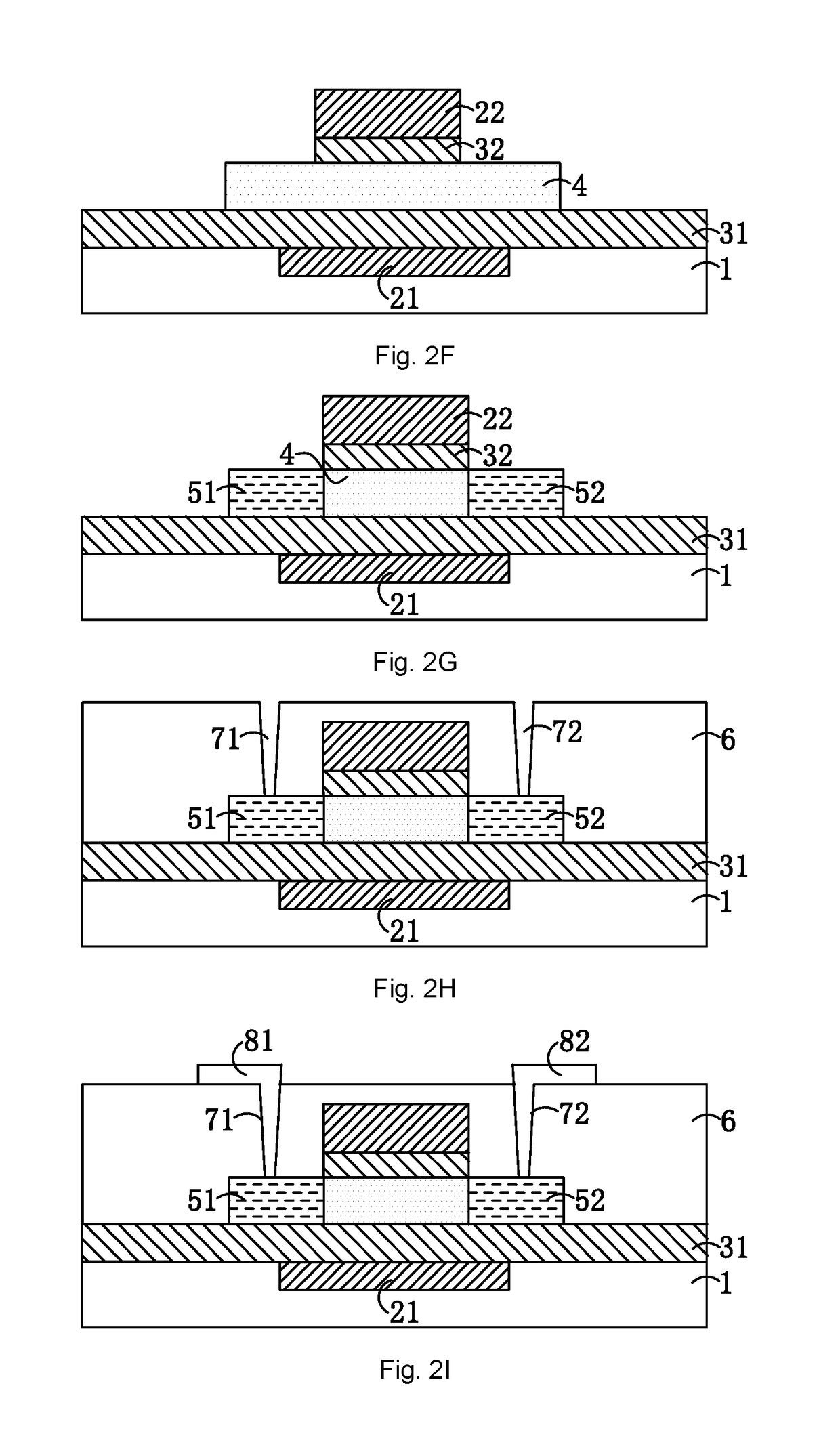
[0086]The present embodiment provides a method of manufacturing a coplanar double gate electrode oxide thin film transistor described in the Embodiment 2, this method differs from the manufacturing method described in Embodiment 2 only in the step of forming the coplanar structure between the patterned bottom gate electrode and the substrate, in particular:

[0087]Preparing a substrate, coating the positive photoresist on the substrate, and exposing and developing, forming the bottom gate electrode pattern on the substrate, removing the substrate not protected by the positive photoresist by the dry etching method or the wet etching method, the substrate is formed with a groove having a depth toward the inside of the substrate, and forming the pattern of the bottom gate electrode in the groove; then immersing the substrate in the de-gumming fluid to remove the positive photoresist.

[0088]Then, forming the patterned bottom gate electrode in the groove, by controlling the dose of the cond...


PUM


Abstract

The present disclosure relates to a coplanar double gate electrode oxide thin film transistor, includes a substrate, a bottom gate electrode, a first gate electrode insulating layer, a oxide semiconductor layer, a source electrode contact area and a drain electrode contact area, a second gate electrode insulating layer and a top gate electrode, wherein, the upper surface of the substrate is recessed toward the inside of the substrate to form a groove, the bottom gate electrode is formed in the groove, so that the upper surface of the bottom gate electrode and the upper surface of the substrate are in the same horizontal plane. The thin film transistor of the present disclosure has the characteristics of the double gate electrode and the coplanar structure, and is capable of improving the stability of the thin film transistor, optimizing the response speed thereof, and lowering the driving voltage.

Description

FIELD OF THE DISCLOSURE[0001]The present disclosure relates to a display technology field, and more particularly to a coplanar double gate electrode oxide thin film transistor and a manufacture method thereof.BACKGROUND OF THE DISCLOSURE[0002]The carrier mobility of the oxide semiconductor is 20 to 30 times that of the amorphous silicon, can greatly increase the charging and discharging rate of the TFT to the pixel electrode, the response speed of the pixels can be improved to achieve faster refresh rate, while a faster response also greatly increases the line scan rate of the pixels, making ultra-high resolution in the TFT-LCD possible. Therefore, the oxide thin film transistor technology is gradually becoming a powerful competitor of the next generation of display technology. However, there is an important constraint on the technology used in mass production of display panels—the stability is not sufficient, therefore, it is necessary to conduct in-depth study of the technology, i...

Claims


Application Information

Patent Timeline
Patent Type & Authority Applications(United States)
IPC IPC(8): H01L29/786H01L29/66H01L21/445H01L27/12
CPCH01L29/78648H01L29/78693H01L29/66969H01L21/445H01L27/1225H01L27/1262H01L27/1292H01L27/127H01L29/78603H01L29/78633H01L21/34H01L29/786
Inventor XIE, YINGTAO
Owner WUHAN CHINA STAR OPTOELECTRONICS TECH CO LTD
Why Eureka
Try Eureka