Light emitting device and method of manufacturing the same

a technology of light emitting devices and manufacturing methods, which is applied in the direction of instruments, mechanical devices, optical elements, etc., can solve the problems of large unevenness in the emission color distribution, and achieve the effects of easy dissipation, reduced unevenness in the emission color distribution, and good productivity

Active Publication Date: 2018-07-26
NICHIA CORP
View PDF11 Cites 22 Cited by
  • Summary
  • Abstract
  • Description
  • Claims
  • Application Information

AI Technical Summary

Benefits of technology

[0008]According to certain embodiments of the present invention, it is possible to obtain a light emitting device in which heat in the fluorescent substance can be easily dissipated and unevenness in the

Problems solved by technology

However, if the phosphor in this region is removed, light emitted from the LED element is emitted toward obliquely above the light emi

Method used


Image

  • Light emitting device and method of manufacturing the same
  • Light emitting device and method of manufacturing the same
  • Light emitting device and method of manufacturing the same

Examples


first embodiment

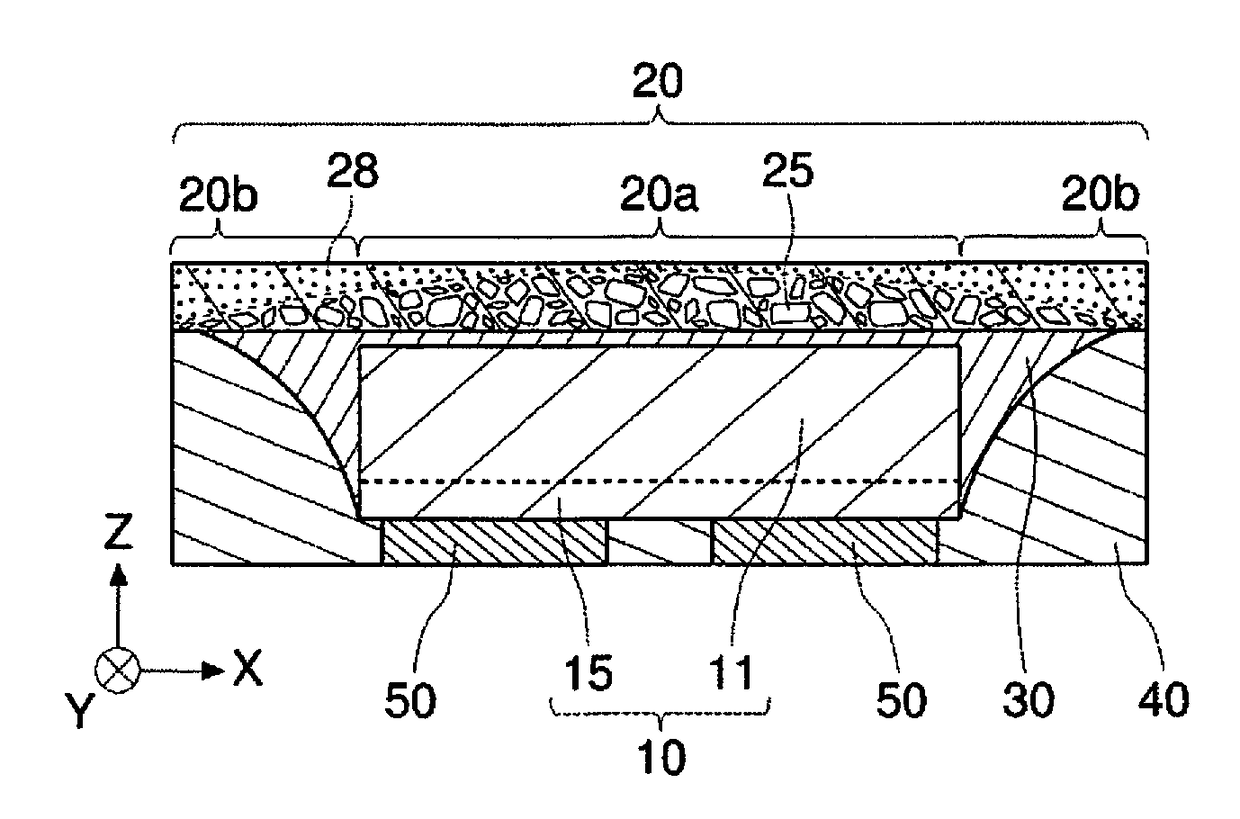
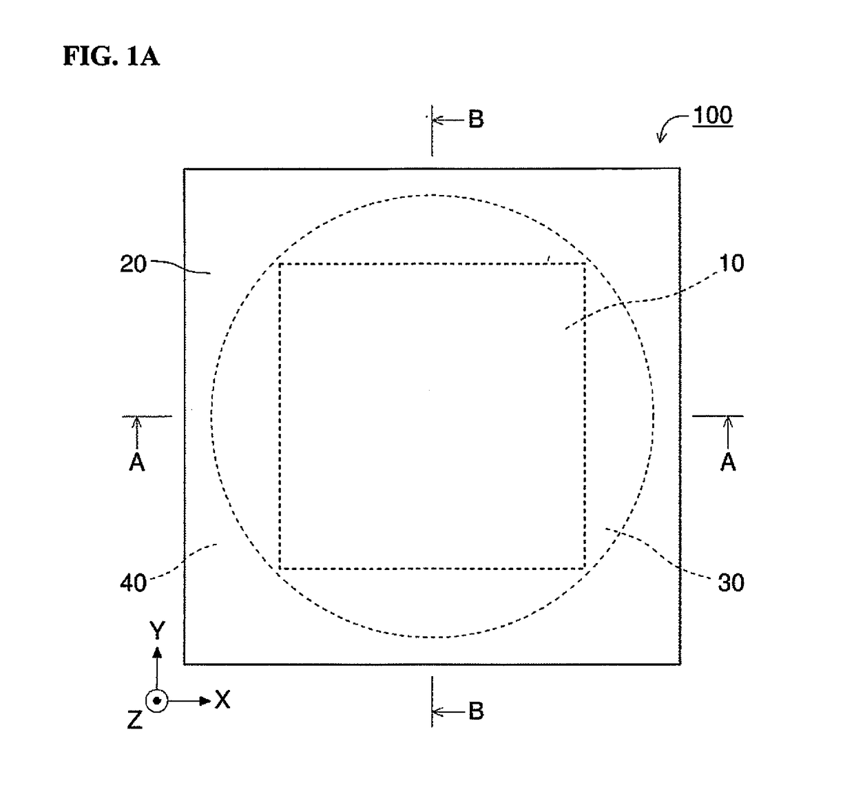
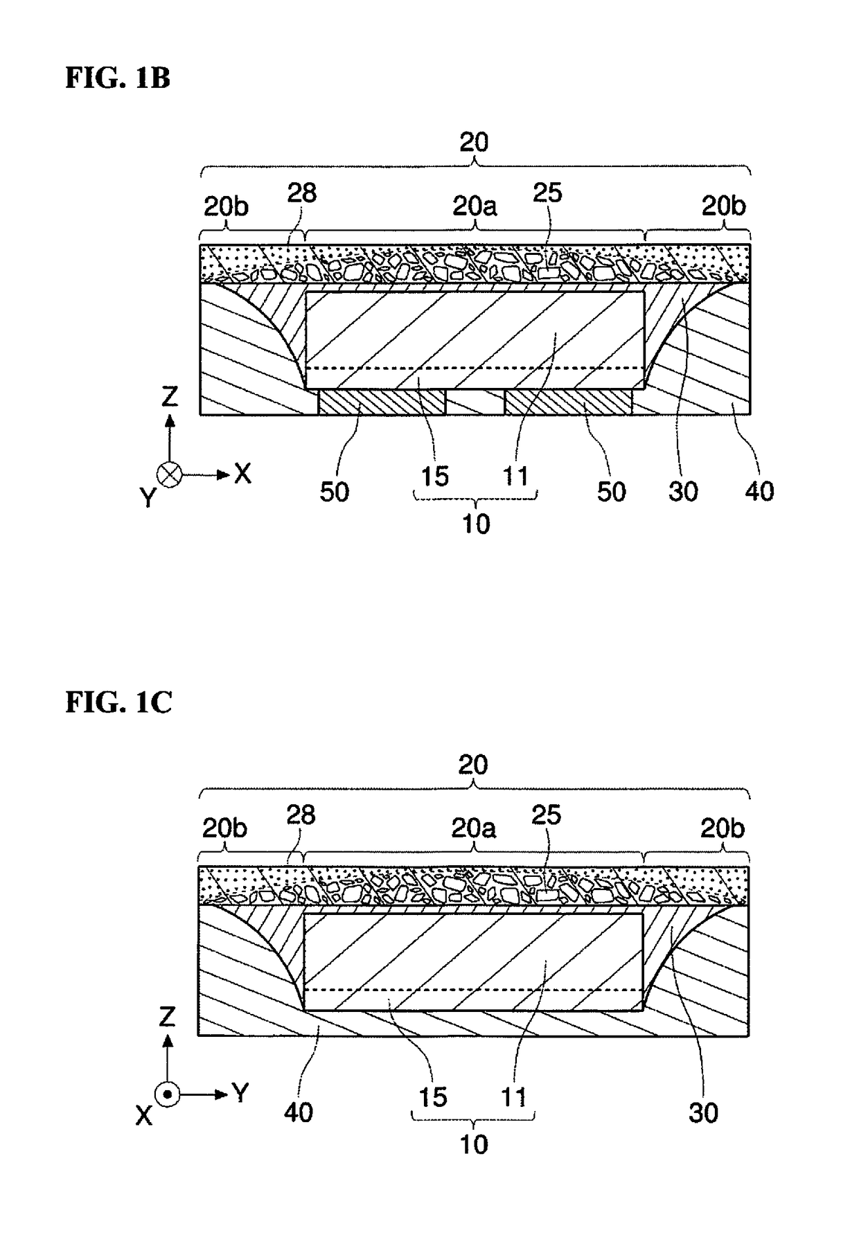
[0027]FIG. 1A is a schematic top view of a light emitting device 100 according to the first embodiment of the present invention. FIG. 1B is a schematic cross sectional view of the light emitting device 100 taken along a line A-A in FIG. 1A. FIG. 1C is a schematic cross section view of the light emitting device 100 taken along a line B-B in FIG. 1A.

[0028]As shown in FIG. 1A to 1C, the light emitting device 100 of the first embodiment includes a light emitting element 10, a light-transmissive member 20, a light guide member 30, and a light reflective member 40. The light-transmissive member 20 is placed above the light emitting element 10. The light-transmissive member 20 comprises a first region 20a positioned directly above a top surface of the light emitting element 10, and a second region 20b at a lateral side of the first region 20a. The light guide member 30 covers the side surface of the light emitting element 10 and a bottom surface of the second region 20b of the light-transm...

second embodiment

[0047]FIG. 3A is a schematic top view of a light emitting device 200 of the second embodiment of the present invention. FIG. 3B is a schematic cross sectional view taken along a line C-C of the light emitting device 200 shown in FIG. 3A. FIG. 3C is a schematic cross sectional view taken along a line D-D of the light emitting device 200 shown in FIG. 3A. Configurations of the light emitting device 200 that differ from the light emitting device 100 of the first embodiment will be described below, and description of configurations substantially the same as that in the light emitting device 100 of the first embodiment will be omitted as appropriate.

[0048]As shown in FIGS. 3B and 3C, in the light emitting device 200 of the second embodiment, a second region 22b includes a fluorescent substance-containing portion 22c and a fluorescent substance-free portion 22d at a lateral side of the fluorescent substance-containing portion 22c. More specifically, the region in the second region 22b in ...

example 1

[0070]The light emitting device of Example 1 is a top surface-emitting CSP type LED device having a rectangular-parallelepiped shape with a width of 1.7 mm, a depth of 1.7 mm, and a thickness of 0.28 mm, and having the structure of the light emitting device 100 of the example shown in FIG. 1A to 1C. The light emitting element 10 is an LED chip of width 1 mm, depth 1 mm, thickness 0.155 mm with a square shape in a top view that can emit blue light at light emission peak wavelength of 455 nm. The light emitting element 10 has a sapphire substrate 11, and a semiconductor layered body 15 in which an n type semiconductor layer of a nitride semiconductor, an active layer, and a p type semiconductor layer are layered in order on the sapphire substrate 11 so as to be in contact with the bottom surface of that substrate 11. The light-transmissive member 20 is disposed above the light emitting element 10 and connected to the light emitting element 10 via the light guide member 30. The light-t...


PUM


Abstract

A light emitting device includes a light emitting element, a light-transmissive member, a light guide member and a light reflective member. The light-transmissive member includes a first region directly above a top surface of the light emitting element, and a second region at a lateral side of the first region. The light guide member covers a lateral surface of the light emitting element and a bottom surface of the second region of the light-transmissive member. The light reflective member covers an outer surface of the light guide member. The light-transmissive member contains a fluorescent substance and a light scattering material that is not a fluorescent substance. A concentration of the fluorescent substance in the light-transmissive member is higher in the first region than in the second region. A concentration of the light scattering material in the light-transmissive member is higher in the second region than in the first region.

Description

CROSS REFERENCE TO RELATED APPLICATIONS[0001]This application claims priority to Japanese Patent Application No. 2017-010533, filed on Jan. 24, 2017. The entire disclosure of Japanese Patent Application No. 2017-010533 is hereby incorporated herein by reference.TECHNICAL FIELD[0002]The present disclosure relates to a light emitting device and a method for manufacturing the same.BACKGROUND ART[0003]For example, in Japanese Laid-Open Patent Application Publication No. 2015-115480, a light emitting device is described that includes: a blue LED element in which a negative electrode and a positive electrode are formed on a bottom surface thereof; a phosphor layer disposed on a top surface of the LED element to emit white light as a whole; reversed square pyramid shaped transparent resin parts disposed on lateral surfaces of the LED element and having a bottom surface on which the phosphor layer is disposed; and a reflecting wall covering exposed surfaces, which are surfaces other than th...

Claims


Application Information

Patent Timeline
IPC IPC(8): H01L33/64F21V8/00H01L33/50H01L33/58H01L33/60H01L33/62
CPCH01L33/644G02B6/0003H01L33/507H01L33/58H01L33/60H01L33/62H01L33/32H01L2933/0091H01L2933/0041H01L2933/0058H01L2933/0075H01L33/508H01L33/54H01L2933/005
Inventor HAYASHI, HIROSUKE
Owner NICHIA CORP
Why Eureka
Try Eureka