Supercharge Your Innovation With Domain-Expert AI Agents!

Stacked image sensor pixel cell with selectable shutter modes and in-pixel cds

a pixel cell and image sensor technology, applied in the field of image sensors, can solve the problems of insufficient total light absorption depth within the substrate, insufficient red light absorption, and insufficient photosensitivity and dynamic range of the pixel, and achieve the effect of reducing the wiring of the pixel

Active Publication Date: 2018-08-09
SMARTSENS TECH (HK) CO LTD
View PDF4 Cites 9 Cited by
  • Summary
  • Abstract
  • Description
  • Claims
  • Application Information

AI Technical Summary

Benefits of technology

The present invention aims to provide a pixel cell that occupies less area, reducing the size of the pixel array and manufacturing cost. Additionally, it includes a stacked pixel with a rolling shutter readout select transistor and a global shutter readout select transistor that have directly connected output terminals to minimize off pixel wiring.

Problems solved by technology

However, miniaturization has come with the loss of pixel photosensitivity and dynamic range which require new approaches in order to mitigate.
With the decreased pixel size, the total light absorption depth within the substrate becomes insufficient for some light, especially long-wavelength light.
This becomes a particular problem for image sensors using backside illumination (BSI) technology wherein the image light is incident upon the backside of the sensor substrate.
In BSI technology the sensor Silicon substrate may be only two microns (micrometers) thick which is adequate to absorb blue light but very inadequate to absorb red light which may require ten microns of thickness to be fully absorbed.
A potential disadvantage of rolling shutter readout mode is spatial distortion which results from the above.
Another disadvantage is that different regions of the exposed image will not be precisely correlated in time and appear as a distortion in the image.
However it carries risk of spatial distortion especially when imaging relatively large, fast moving objects.

Method used


Image

  • Stacked image sensor pixel cell with selectable shutter modes and in-pixel cds
  • Stacked image sensor pixel cell with selectable shutter modes and in-pixel cds
  • Stacked image sensor pixel cell with selectable shutter modes and in-pixel cds

Examples


Embodiment Construction

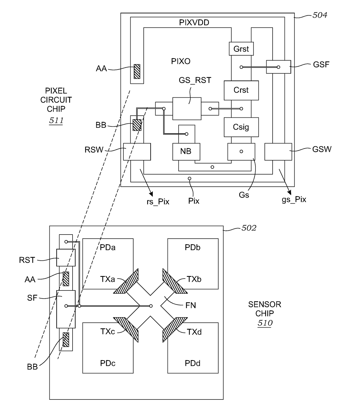
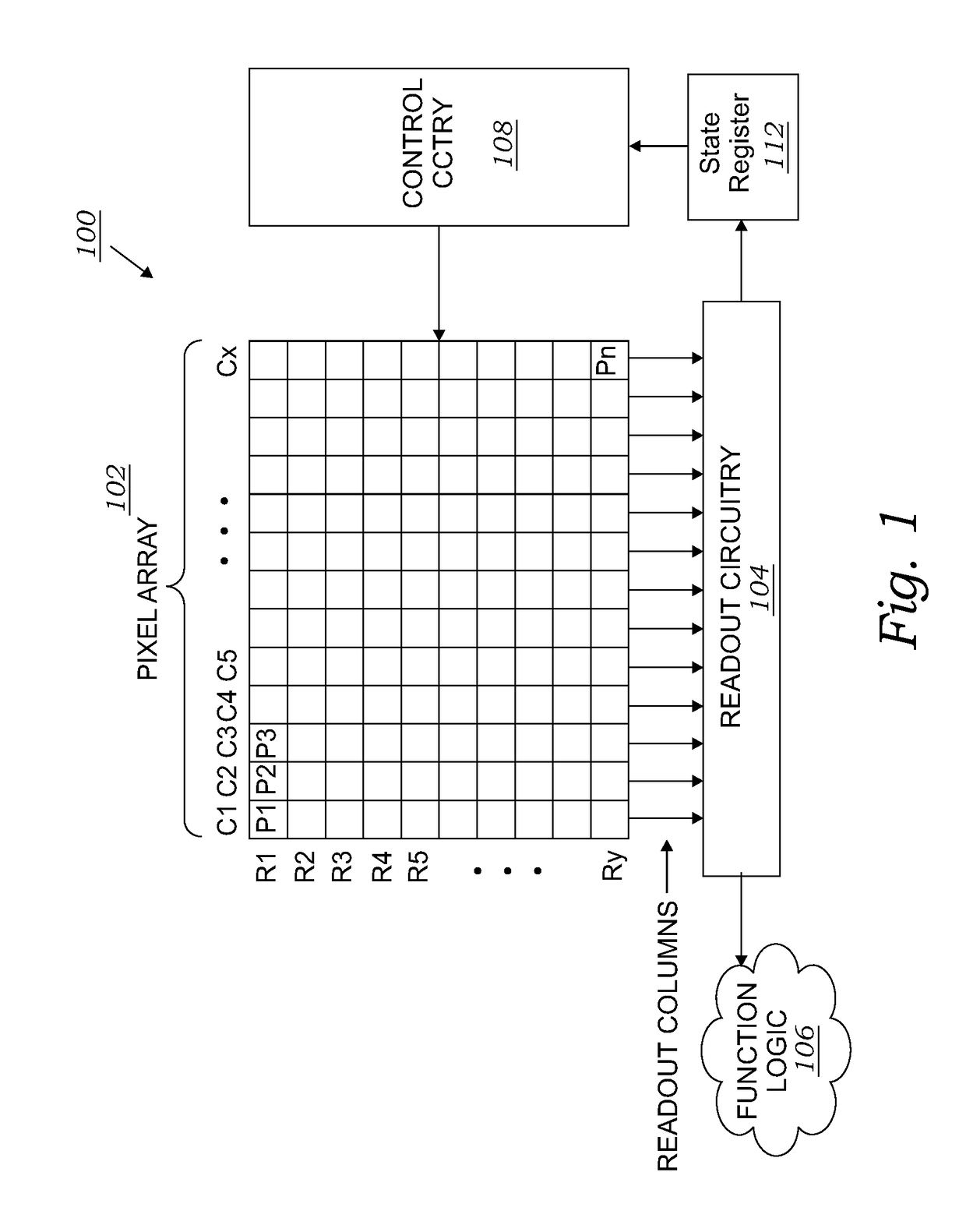
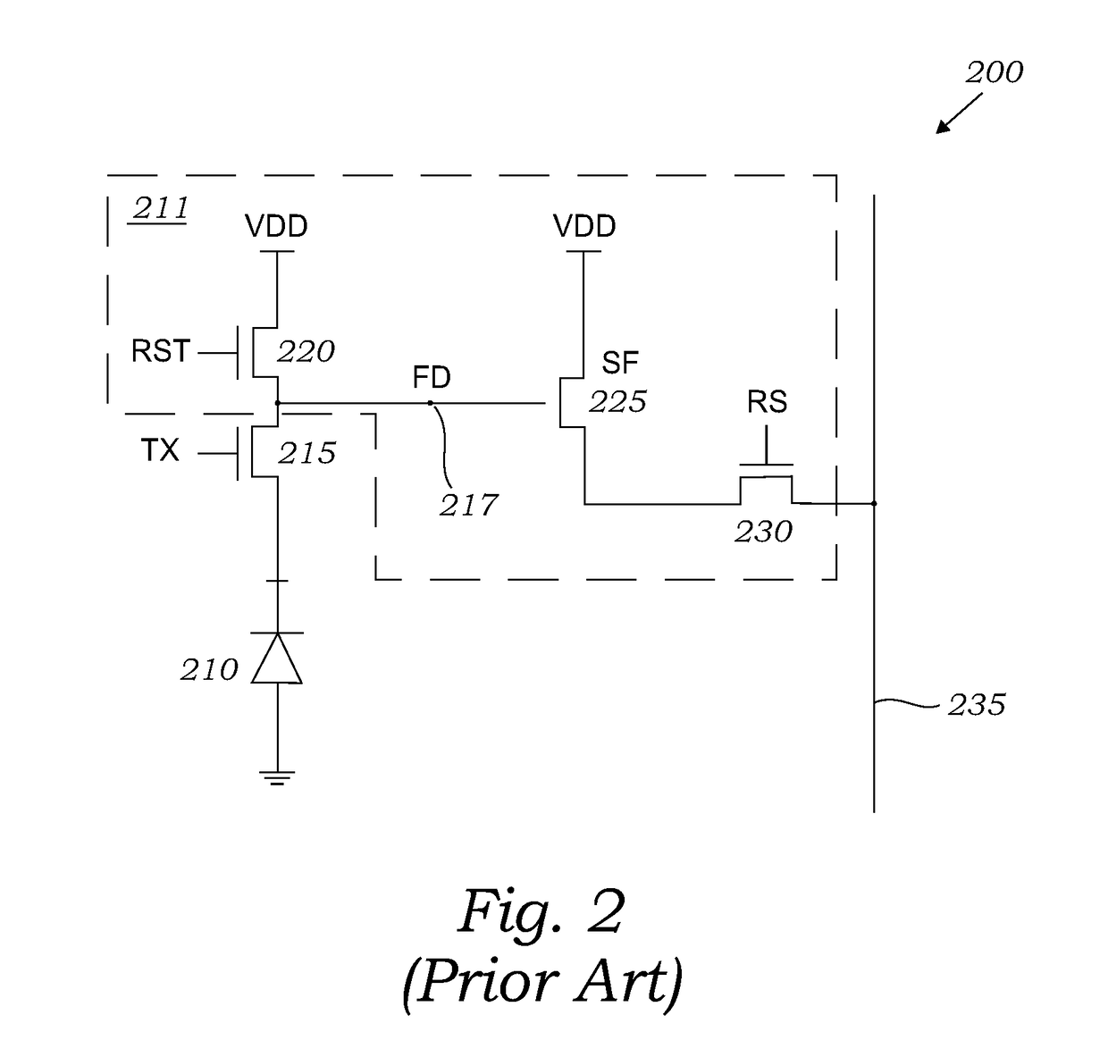
[0035]The above-described drawing figures illustrate the invention, a stacked image sensor pixel cell with optionally selectable rolling shutter and global shutter readout modes and in-pixel CDS in the global shutter readout path. Various embodiments of the stacked image sensor are disclosed herein. In the following description, numerous specific details are set forth in order to provide a thorough understanding of the present invention. One skilled in the relevant art will recognize, however, that the techniques described herein can be practiced without one or more of the specific details, or with other methods, components, materials, etc. In other instances, well-known structures, materials, or operations are not shown or described in detail to avoid obscuring certain aspects. A substrate may have a front side and a back side. Any fabrication process that is performed from the front side may be referred to as a frontside process while any fabrication process that is performed from...


PUM


Abstract

A pixel cell has a photodiode, a transfer transistor, a reset transistor, an amplifier transistor and a readout circuit block. The photodiode, transfer transistor, reset transistor and amplifier transistor are disposed within a first substrate of a first semiconductor chip for accumulating an image charge in response to light incident upon the photodiode and converting the image charge to an image signal. The readout circuit block is disposed within a second substrate of a second semiconductor chip and the readout circuit block comprises optionally selectable rolling shutter and global shutter readout modes through the use of computer programmable digital register settings. The global shutter readout mode provides in-pixel correlated double sampling.

Description

CROSS-REFERENCE TO RELATED APPLICATIONS[0001]This application for a utility patent is a continuation-in-part of a previously filed utility patent, still pending, having the application Ser. No. 15 / 424,124, filed 3 Feb. 2017 and application Ser. No. 15 / 609,857, filed 31 May 2017.BACKGROUND OF THE INVENTIONField of the Invention[0002]This invention relates generally to image sensors, and more particularly to CMOS image sensors in a stacked chip formation. The bottom chip includes an array of light sensitive regions and structures to capture an image. The top chip includes circuit elements to extract an image from the array. The image sensor may be incorporated within a digital camera.Description of Related Art[0003]An image capture device includes an image sensor and an imaging lens. The imaging lens focuses light onto the image sensor to form an image, and the image sensor converts the light into electrical signals. The electric signals are output from the image capture device to oth...

Claims


Application Information

Patent Timeline
Patent Type & Authority Applications(United States)
IPC IPC(8): H04N5/378H04N5/374H01L27/146
CPCH04N5/378H04N5/374H01L27/14634H01L27/1469H01L27/14621H01L27/14645H01L27/14636H04N23/54H04N23/70H04N25/76H04N25/78H04N25/616H04N25/771H04N25/778H04N25/65H04N25/75
Inventor MO, YAOWU PINGXU, CHENSHAO, ZEXU
Owner SMARTSENS TECH (HK) CO LTD
Features
  • R&D
  • Intellectual Property
  • Life Sciences
  • Materials
  • Tech Scout
  • Unparalleled Data Quality
  • Higher Quality Content
  • 60% Fewer Hallucinations
Learn More