Semiconductor device, light emission control circuit, and electronic appliance

a technology of light emission control circuit and semiconductor device, which is applied in the direction of optics, instruments, electroluminescent light sources, etc., can solve the problems of noise or electric power consumption increase, the gate voltage rise time is delayed with respect to the pwm signal, and the inability to achieve highly accurate digital dimming, etc., to achieve accurate adjustment of the brightness level of the light emitting element, reduce the number of capacitors, and achieve high-quality digital dimming.

Active Publication Date: 2018-09-20
SEIKO EPSON CORP
View PDF6 Cites 12 Cited by
  • Summary
  • Abstract
  • Description
  • Claims
  • Application Information

AI Technical Summary

Benefits of technology

[0006]Thus, in view of the above-described points, a first advantage of some aspects of the invention is to provide a semiconductor device and a light emission control circuit, with which it is possible to achieve highly accurate digital dimming by reducing the rise time or the fall time of the gate voltage of a switching transistor without increasing noise or electric power consumption when a light emitting element is PWM driven for digital dimming. Furthermore, a second advantage of some aspects of the invention is to provide an electronic appliance or the like that includes such a light emission control circuit.
[0008]According to the first aspect of the invention, the second control signal output from the second driving circuit is supplied to the gate of the transistor that controls the electric current that flows through the light emitting element via the capacitor. With this configuration, the waveform of the gate voltage of the switching transistor can be improved without increasing the driving ability of the first driving circuit. It is therefore possible to achieve highly accurate digital dimming by reducing the rise time or the fall time of the gate voltage of the switching transistor without increasing noise or electric power consumption when the light emitting element is PWM driven for digital dimming.
[0010]In this case, the first driving circuit may generate the first control signal that has an amplitude substantially equal to an amplitude of the second control signal. With this configuration, the rise time or the fall time of the gate voltage of the switching transistor can be shortened while balancing between the driving ability of the first driving circuit and the driving ability of the second driving circuit.
[0013]A light emission control circuit according to a second aspect of the invention includes: a transistor that controls an electric current that flows through a light emitting element; a capacitor that includes one end connected to a gate of the transistor, and has a capacitance larger than a capacitance of the gate of the transistor; and any one of the semiconductor devices described above that controls the transistor. According to the second aspect of the invention, the second control signal generated by the second driving circuit can be supplied efficiently to the gate of the switching transistor.
[0015]According to the third aspect of the invention, in the light emission control circuit that includes a plurality of semiconductor devices for controlling the light emission operations of a plurality of light emitting elements, the third and fourth power supply potentials that are respectively generated by the first and second regulators of one semiconductor device are shared among the plurality of semiconductor devices, and therefore the third and fourth power supply potentials used in the plurality of semiconductor devices can be uniform, and reduce the number of capacitors that smooth the third and fourth power supply potentials.
[0016]An electronic appliance according to a fourth aspect of the invention includes: a light emitting element, or a first light emitting element and a second light emitting element; and the light emission control circuit according to the second or third aspect of the invention that controls a light emission operation of the light emitting element, or light emission operations of the first light emitting element and the second light emitting element. According to the fourth aspect of the invention, it is possible to provide an electronic appliance that can accurately adjust the brightness level of the light emitting element by using the light emission control circuit that can achieve highly accurate digital dimming without increasing noise or electric power consumption when the light emitting element is PWM driven for digital dimming.

Problems solved by technology

However, due to the gate-to-source capacitance of a transistor for digital dimming, the rise time of the gate voltage delays with respect to the PWM signal.
Accordingly, when the pulse width of the PWM signal is small, highly accurate digital dimming cannot be achieved due to the influence of an error in the pulse width.
On the other hand, in order to shorten the rise time or the fall time of the gate voltage, if the driving ability of a driving circuit that drives the transistor for digital dimming, or the electric current supplying ability of a regulator that supplies a power supply potential to the driving circuit is increased, noise or electric power consumption increases.

Method used


Image

  • Semiconductor device, light emission control circuit, and electronic appliance
  • Semiconductor device, light emission control circuit, and electronic appliance
  • Semiconductor device, light emission control circuit, and electronic appliance

Examples


first embodiment

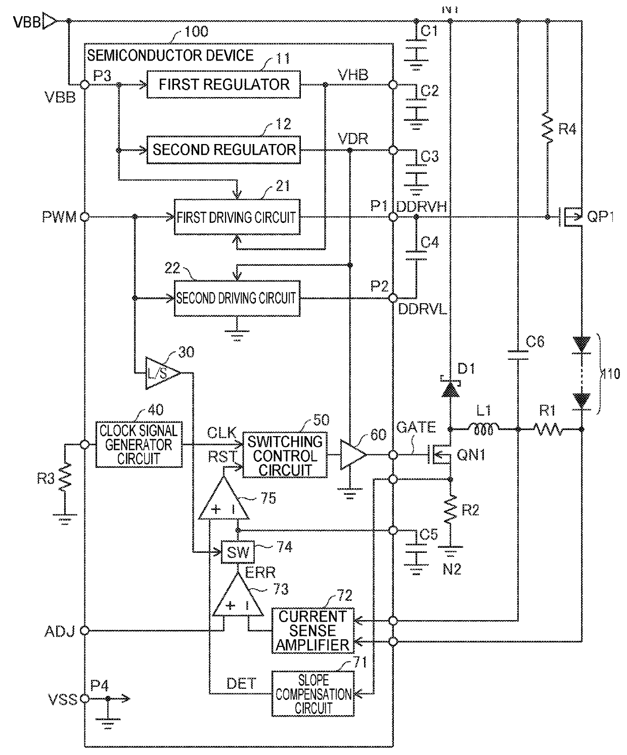
[0057]In a first embodiment, the first driving circuit 21 activates or deactivates the first control signal DDRVH based on the digital dimming signal PWM in phase with the second control signal DDRVL. With this configuration, the gate of the transistor QP1 that controls the electric current that flows through the light emitting element 110 is driven by the second driving circuit 22 via the capacitor C4, and also driven by the first driving circuit 21 in the same phase. Accordingly, the rise time or the fall time of the gate voltage of the transistor QP1 can be shortened as compared with the configuration in which it is driven by one driving circuit. Although there is a possibility that one of the first control signal DDRVH and the second control signal DDRVL might delay with respect to the other due to the parasitic capacitance of a transmission path or the like, such a phase difference is permissible.

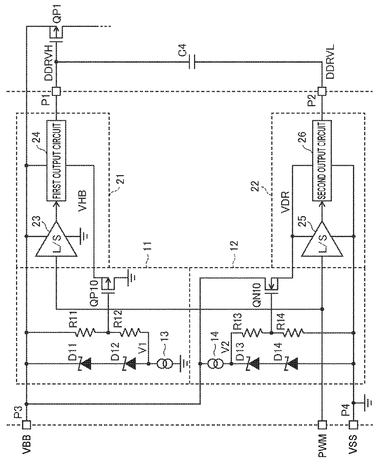
[0058]FIG. 2 is a circuit diagram showing a configuration example of a portion of ...

second embodiment

[0086]In a second embodiment, the first driving circuit 21 shown in FIG. 1 outputs the first control signal DDRVH to the first terminal P1 so as to charge the capacitor C4 at the time when the semiconductor device 100 is powered on or the like (hereinafter referred to as “at the time of startup”), and supplements electric charges to the capacitor C4 during the subsequent normal operation.

[0087]FIG. 6 is a circuit diagram showing a configuration example of a portion of a semiconductor device according to a second embodiment of the invention. The second embodiment is configured by replacing the first regulator 11 and the first driving circuit 21 of the first embodiment shown in FIG. 2 with a first regulator 11a and a first driving circuit 21a, and adding a startup circuit 80 and an N-channel MOS transistor QN80. Other than the above, the second embodiment may be configured in the same manner as the first embodiment.

[0088]As shown in FIG. 6, in the first regulator 11a, a resistor R15 i...

third embodiment

[0096]In a third embodiment, a method similar to the method for shortening the rise time or the fall time of the gate voltage of the transistor QP1 for digital dimming according to the first embodiment is used to shorten the rise time or the fall time of the gate voltage of the transistor QN1 for analog dimming.

[0097]FIG. 7 is a circuit diagram showing a configuration example of a portion of a semiconductor device according to a third embodiment of the invention. In the third embodiment, a drive circuit 60a is used instead of the drive circuit 60 shown in FIG. 1. Other than the above, the third embodiment may be configured in the same manner as the first or second embodiment.

[0098]The drive circuit 60a includes inverters 61 and 62, a diode D60, a P-channel MOS transistor QP60, and an N-channel MOS transistor QN60. An external capacitor C7 is connected between the source of the transistor QP60 and the source of the transistor QN60 via two terminals P5 and P6 of the semiconductor devi...


PUM


Abstract

A semiconductor device of the invention is a semiconductor device that controls a transistor that controls an electric current that flows through a light emitting element, the transistor including a gate that is connected to one end of a capacitor. The semiconductor device includes: a first terminal that is connected to the gate of the transistor and the one end of the capacitor; a second terminal that is connected to the other end of the capacitor; a first driving circuit that outputs a first control signal to the first terminal; and a second driving circuit that, in order to control the transistor in an on-state or an off-state, activates or deactivates a second control signal, and outputs the second control signal to the second terminal, the second control signal having a potential lower than a potential of the first control signal.

Description

BACKGROUND1. Technical Field[0001]The present invention relates to a semiconductor device and a light emission control circuit that control a light emission operation of a light emitting element such as a light emitting diode (LED). Furthermore, the invention also relates to an electronic appliance or the like that includes such a light emission control circuit.2. Related Art[0002]As techniques for adjusting the brightness level of a light emitting element such as an LED, digital dimming and analog dimming are known. For example, the digital dimming is implemented by adjusting the length of a period in which an electric current flows through the light emitting element by performing control so as to turn on or off a switching transistor connected in series to the light emitting element. On the other hand, the analog dimming is implemented by adjusting the magnitude of an electric current that flows through the light emitting element by controlling a switching power supply or the like...

Claims


Application Information

Patent Timeline
Patent Type & Authority Applications(United States)
IPC IPC(8): G03B21/20H05B37/02H05B33/08H05B44/00
CPCG03B21/2053H05B37/0209G03B21/2033H05B33/0818H05B33/0851H05B45/10H05B45/3725Y02B20/40
Inventor YAMADA, ATSUSHI
Owner SEIKO EPSON CORP
Why Eureka
Try Eureka