

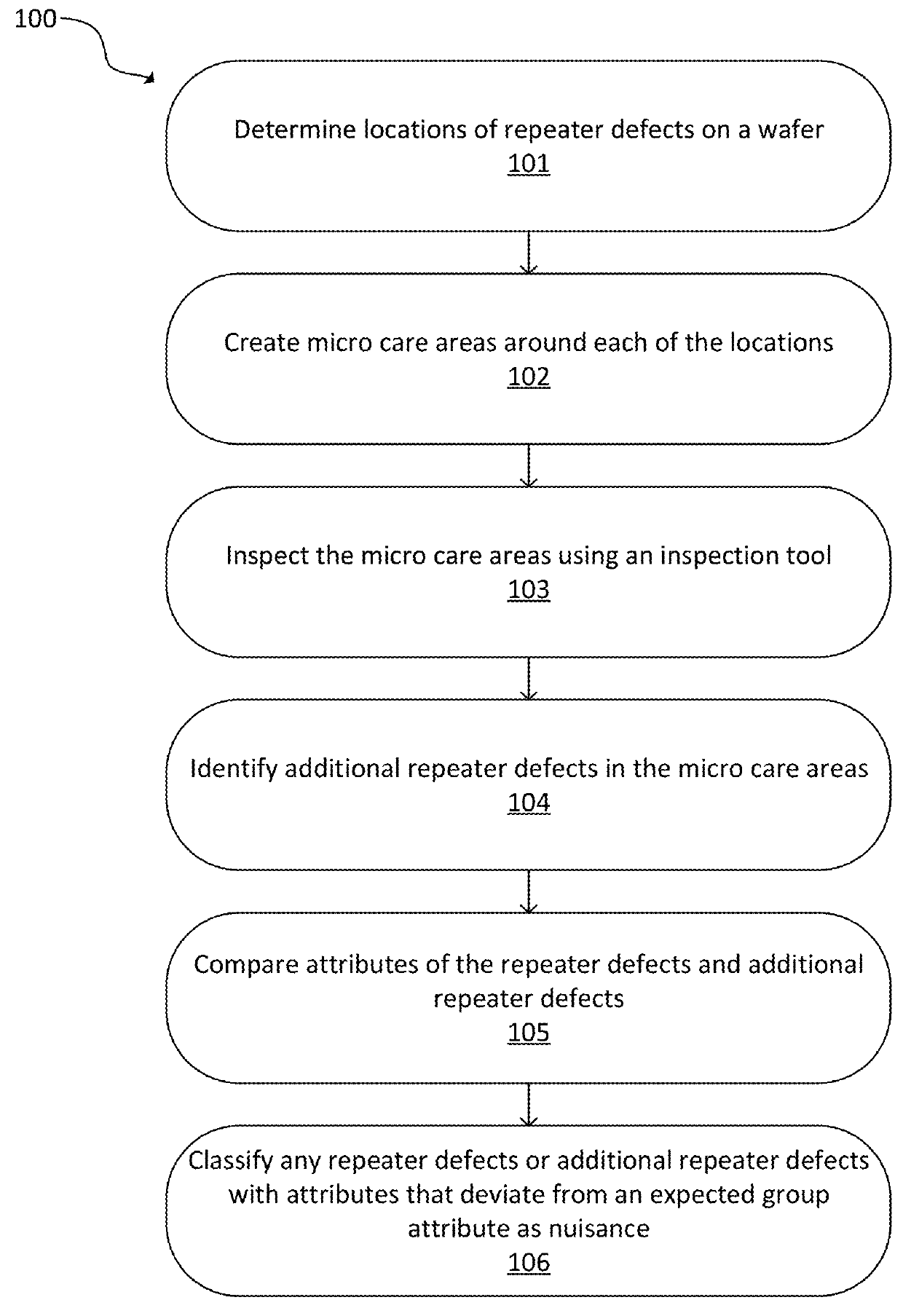
Dynamic Care Areas for Defect Detection
- Summary
- Abstract
- Description
- Claims
- Application Information
AI Technical Summary
Benefits of technology
Problems solved by technology
Method used
Image

Examples
first embodiment
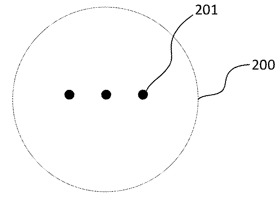
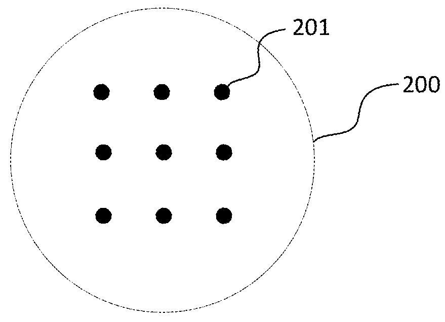
[0083]FIG. 5 is nuisance reduction. A first die and a second die are each imaged using a reticle at two different positions (reticle1, reticle2) on a first wafer (t=0) and two different positions (reticle1, reticle2) on a second wafer (t>0). The two different positions may be, for example, different rows on the wafer. The first die and the second die may be neighboring dies or may have other spatial relationships. The image processing steps may be performed by a processor.
[0084]A first wafer difference image is calculated. To do so, a difference image of the first die and the second die at a second position on the first wafer is calculated. A difference image of the first die at the second position on the first wafer and the second die at a first position on the first wafer also is calculated. Then the first wafer difference image is calculated from the two resulting difference images.
[0085]A second wafer difference image is calculated. To do so, a difference image of the first die ...
second embodiment
[0087]FIG. 6 is nuisance reduction. A first die and a second die are each imaged using a reticle at two different positions (reticle1, reticle2) on a first wafer (t=0) and two different positions (reticle1, reticle2) on a second wafer (t>0). The two different positions may be, for example, different rows on the wafer. The first die and the second die may be neighboring dies or may have other spatial relationships. The image processing steps may be performed by a processor.
[0088]A difference image of the first die and the second die at a second position on the second wafer is calculated. A difference image of the first die at the second position on the first wafer and the second die at a first position on the second wafer is calculated. Then a wafer difference image is calculated from the two resulting difference images.
[0089]Existence of a defect of interest in the wafer difference image is determined. Images can be retrieved from the storage medium. The images are at the same locat...
third embodiment
[0090]FIG. 7 is nuisance reduction. A first die and a second die are each imaged using a reticle at two different positions (reticle1, reticle2) on a first wafer (t=0) and two different positions (reticle1, reticle2) on a second wafer (t>0). The two different positions may be, for example, different rows on the wafer. The first die and the second die may be neighboring dies or may have other spatial relationships. The image processing steps may be performed by a processor.
[0091]A first wafer difference image is calculated. To do so, a difference image of the first die and the second die at a second position on the first wafer is calculated. A difference image of the first die at the second position on the first wafer and the second die at a first position on the first wafer also is calculated. Then the first wafer difference image is calculated from the two resulting difference images.
[0092]A second wafer difference image is calculated. To do so, a difference image of the first die ...
PUM
 Abstract
Description
Claims
Application Information