Wide band gap device integrated circuit architecture on engineered substrate

a technology of integrated circuits and substrates, which is applied in the direction of semiconductor/solid-state device manufacturing, semiconductor devices, electrical apparatus, etc., can solve the problems of wbg semiconductor devices that are expensive and time-consuming to manufacture, negatively affecting device yield and performance, and cracks or delaminate gans, etc., to reduce stress, improve dislocation density, and improve electrical and optical properties of epitaxial layers.

Active Publication Date: 2018-10-04
QROMIS INC
View PDF9 Cites 0 Cited by
  • Summary
  • Abstract
  • Description
  • Claims
  • Application Information

AI Technical Summary

Benefits of technology

[0007]Numerous benefits can be achieved by way of the present invention over conventional techniques. For example, embodiments of the present invention provide solid state devices, such as light-emitting diodes (LEDs) or high electron mobility transistors (HEMTs), formed on engineered substrates that have a CTE that is substantially matched to the CTE of the epitaxial layers of the solid state devices. Matching the thermal expansion properties of the growth substrate to the epitaxial layer reduces the stress in the epitaxial layers and / or the engineered substrate. Stress is responsible for several types of defects. For example, stress may increase dislocation density in the epitaxial layer, which may impair electrical and optical properties of the epitaxial layer. Stress may also lead to residual strain in the epitaxial layer or the substrate, which may lead to additional processing concern in later steps, such as stress cracking, dislocation glide, slip, bow, and warp. Thermal expansion induced bow and warp of the substrate may make handling of the material problematic in automated equipment, and may limit the ability to perform additional lithographic steps necessary for device fabrication. In addition, the device performance lifetime may be reduced in stressed materials. Stress relaxation and stress-induced crack propagation, dislocation glide, and other lattice movement resulting from thermal mismatch may lead to early failures in a range of modes, from reduced device performance to fracture or peeling of devices and device layers.
[0008]Embodiments of the present invention provide methods and techniques for fabricating high density, low cost WBG integrated circuits using a large engineered substrate having a CTE that matches the CTE of the WBG epitaxial layer. Because the CTE match, a thicker epitaxial layer may be formed. The thicker epitaxial layer may reduce the overall dislocation density of the lattice structures of the epitaxial layer, and thus may improve the performance and reliability of integrated circuits manufactured using the thick epitaxial layer. Furthermore, the thicker epitaxial layer may allow more devices to be integrated in each unit area, and therefore may increase the device density, reduce the size of each integrated circuit, and / or allow more complex circuitry to be manufactured. Because the size of each integrated circuit may be reduced and a large substrate can be used, more integrated circuits may be made on one substrate. In addition, the engineered substrate may be separated from the manufactured integrated circuits and be reused to grow new epitaxial layers. Therefore, the overall cost of each integrated circuit may be reduced significantly.

Problems solved by technology

Wide band gap (WBG) semiconductor devices are expensive and time consuming to manufacture.
The lattice mismatch between the GaN and the carrier substrate may create defects, dislocations, and strains that may negatively impact device yields and performance.
Thermal processing (e.g., GaN epitaxial growth) can crack or delaminate the GaN, or bow and, in some cases, break the carrier substrate.
The different CTEs may restrict substrate wafer size, limiting scale and preventing reduction of the overall manufacturing cost of WBG devices and solutions.

Method used


Image

  • Wide band gap device integrated circuit architecture on engineered substrate
  • Wide band gap device integrated circuit architecture on engineered substrate
  • Wide band gap device integrated circuit architecture on engineered substrate

Examples


example integrated

Circuit and Its Fabrication

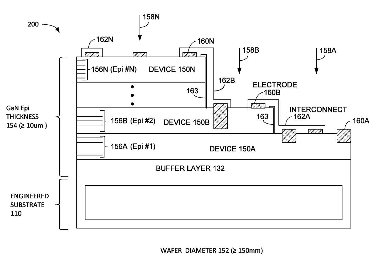
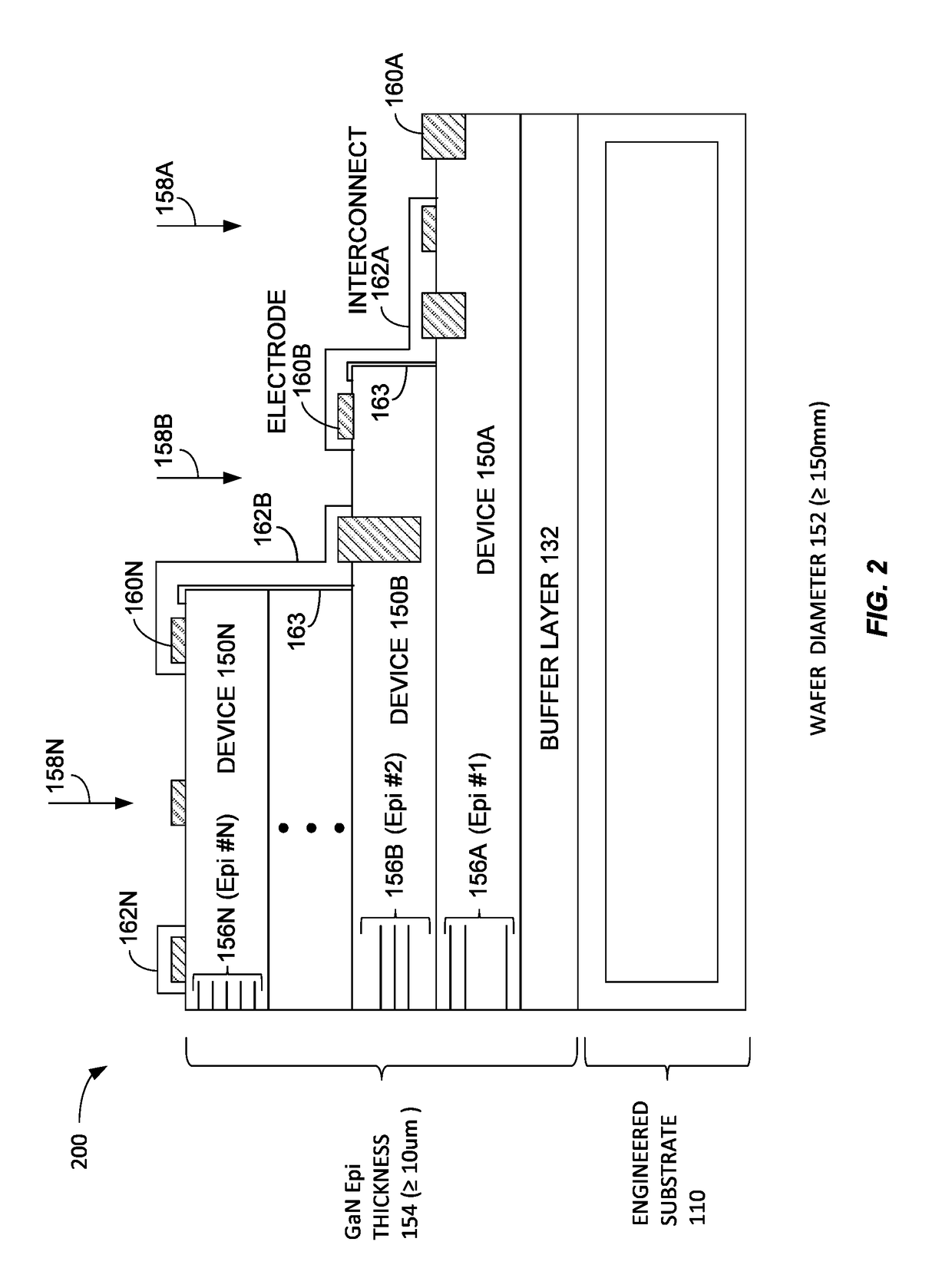
[0038]FIG. 3 shows one example integrated circuit 300 formed on an engineered substrate using GaN epitaxial layers 156 shown in FIG. 2. In this example, the group of epitaxial layers for GaN device 150A may form a wide band gap (WBG) filed effect high electron mobility transistor (HEMT), and the group of epitaxial layers for GaN device 150B may form a light emitting diode (LED). The HEMT (GaN device 150A) includes a source 170, a gate 172, and a drain 174. The LED (GaN device 150B) includes an n-doped cathode 178 and a p-doped anode 176 connected to drain 174 of the HEMT (GaN device 150A).

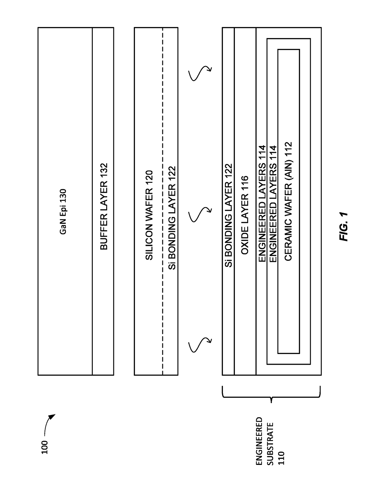
[0039]FIG. 4 shows different GaN layers used for different GaN device in an example GaN epitaxial layer 130 for forming integrated circuit 300 of FIG. 3. Again, this is just one example, and other architectures may also form the HEMT (GaN device 150A) and the LED (GaN device 150B). A typical group of epitaxial layers for the HEMT may include an undoped GaN layer 180 forme...


PUM


Abstract

A method includes forming a wide band gap (WBG) epitaxial layer on an engineered substrate. The WBG epitaxial layer includes a plurality of groups of epitaxial layers. The engineered substrate includes engineered layers formed on a bulk material having a coefficient of thermal expansion (CTE) matching a CTE of the WBG epitaxial layer. The method also includes forming a plurality of WBG devices based on the plurality of groups of epitaxial layers by: for each respective WBG device, forming internal interconnects and electrodes within a respective group of epitaxial layers. The method further includes forming external interconnects between the electrodes of different WBG devices of the plurality of WBG devices to form an integrated circuit.

Description

CROSS-REFERENCES TO RELATED APPLICATIONS[0001]This application is a divisional application of U.S. patent application Ser. No. 15 / 367,108, filed on Dec. 1, 2016, which claims the benefit of U.S. Provisional Patent Application No. 62 / 263,462, filed on Dec. 4, 2015, the contents of which are incorporated herein by reference in their entirety for all purposes.BACKGROUND OF THE INVENTION[0002]Wide band gap (WBG) semiconductor devices are expensive and time consuming to manufacture. For example, gallium nitride (GaN) materials may be formed by a heteropitaxial (epi) growth process that involves depositing GaN on a semiconductor carrier substrate having a different lattice structure (or lattice constant) than the deposited GaN. The lattice mismatch between the GaN and the carrier substrate may create defects, dislocations, and strains that may negatively impact device yields and performance. In addition, the GaN layers and carrier substrate may have different coefficients of thermal expan...

Claims


Application Information

Patent Timeline
Patent Type & Authority Applications(United States)
IPC IPC(8): H01L27/15H01L33/32H01L33/06H01L33/00H01L29/778H01L21/02H01L29/20H01L21/306H01L21/285H01L29/417
CPCH01L29/7786H01L29/41766H01L29/2003H01L21/28575H01L21/30612H01L21/02389H01L33/32H01L33/0075H01L33/06H01L21/0254H01L29/7787H01L27/15H01L33/007H01L29/66431
Inventor ODNOBLYUDOV, VLADIMIRBASCERI, CEM
Owner QROMIS INC
Why Eureka
Try Eureka