Check patentability & draft patents in minutes with Patsnap Eureka AI!

Crossbar resistive memory array with highly conductive copper/copper alloy electrodes and silver/silver alloys electrodes

a resistive memory and crossbar technology, applied in the field of resistive random access memory, can solve problems such as rram generation defects in thin oxide layers

Active Publication Date: 2018-10-04
IBM CORP
View PDF2 Cites 1 Cited by
  • Summary
  • Abstract
  • Description
  • Claims
  • Application Information

AI Technical Summary

Benefits of technology

The present invention provides a method for depositing layers on a silicon surface, specifically using atomic layer deposition (ALD) to grow large crystal grains in the first metal film and in the second metal film. This method allows for better crystal quality and reduced defects in the resulting device. An apparatus based on this method is also provided. Technical effects include improved device performance and reliability.

Problems solved by technology

RRAM generates defects in a thin oxide layer.

Method used


Image

  • Crossbar resistive memory array with highly conductive copper/copper alloy electrodes and silver/silver alloys electrodes
  • Crossbar resistive memory array with highly conductive copper/copper alloy electrodes and silver/silver alloys electrodes
  • Crossbar resistive memory array with highly conductive copper/copper alloy electrodes and silver/silver alloys electrodes

Examples


Embodiment Construction

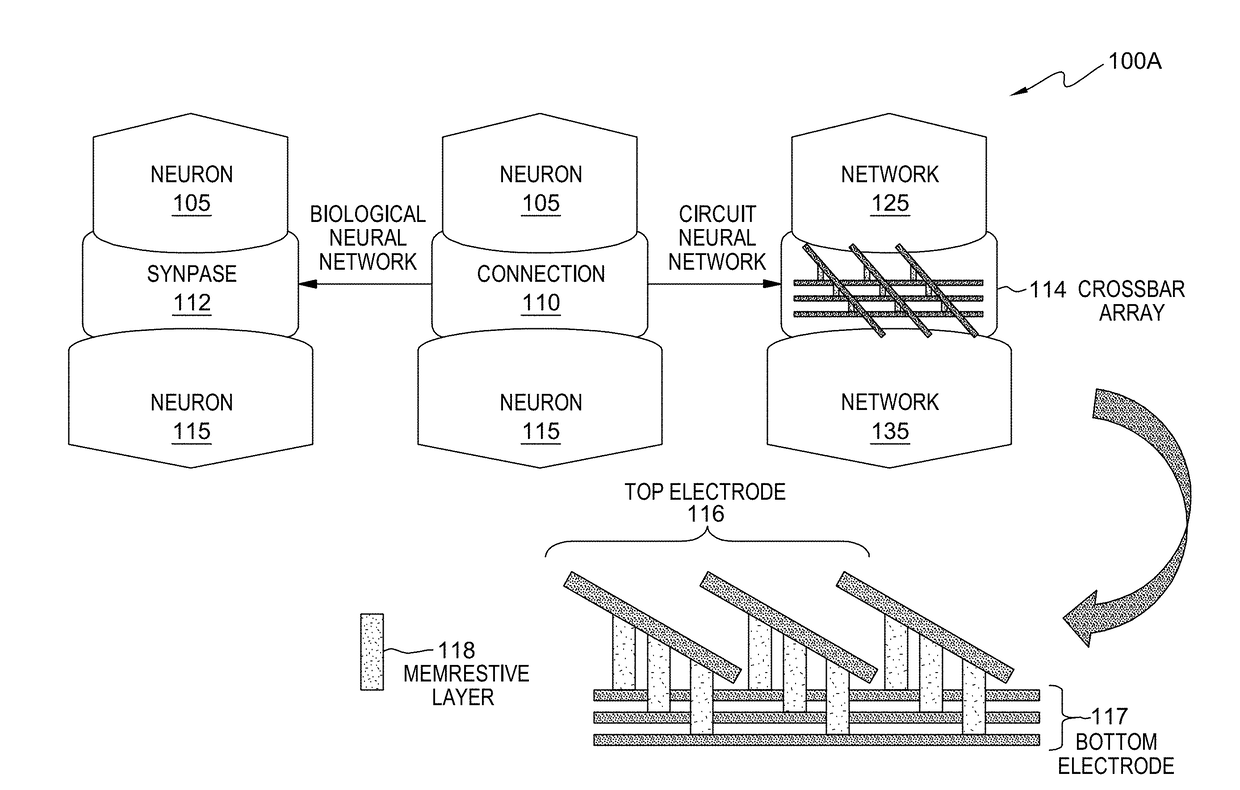
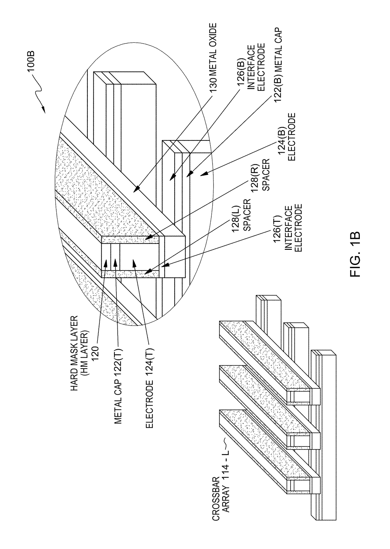
[0014]Neuromorphic computing is directed towards the use of very-large-scale integration (VLSI) systems containing electronic analog circuits to mimic neuro-biological architectures present in the nervous system. RRAM is considered as a promising technology for electronic synapse devices or memristors for neuromorphic computing as well as high-density and high-speed non-volatile memory applications. The methods and systems of the present invention enable the coexistence of highly conductive electrodes and a small active area (i.e., 4F2, where F is the minimum feature size accessible by lithography within a RRAM cell). More specifically, a novel crossbar array structure with a highly conductive electrode and large grains (i.e., crystallites or microscopic crystals within a material) provide lower line resistivity at a smaller line width. Furthermore, embodiments of the present invention enable the contact area of crossbar array structure to be relatively small (e.g., 4F2) relative to...


PUM


Abstract

Embodiments of the present invention provide systems and methods for the fabrication of a crossbar array fabrication of resistive random access memory (RRAM) cells. The array structure contains large grain copper and its alloy or silver and its alloy. A metal cap and spacer are used to protect copper or silver from chemical modifications during memory cell patterning.

Description

BACKGROUND[0001]The present invention relates generally to the field of circuit materials, and more particularly to resistive random access memory (RRAM).[0002]RRAM is a type of non-volatile random-access computer memory that changes the resistance across a dielectric solid-state material (e.g., a memresistor). RRAM generates defects in a thin oxide layer. These defects are oxygen vacancies (i.e., oxide bond locations where the oxygen has been removed) and can be charged and drifted under an electric field. Within RRAM cells, dielectrics (which are typically insulating materials) can be made into conducting materials through a metallic filament or conducting path formed after the application of a sufficiently high voltage. Reported RRAM systems have utilized different dielectric materials (e.g., perovskites, transition metal oxides, chalcogenides, organic charge-transfer complexes, organic donor-acceptor systems, and two dimensional insulating nitrides). A created filament may be re...

Claims


Application Information

Patent Timeline
IPC IPC(8): H01L45/00G06N3/04H01L27/24
CPCG06N3/04H01L27/2463H01L45/146H01L45/1691H01L45/1233H01L45/085H01L45/1253G06N3/063H10B63/80H10N70/24H10N70/841H10N70/826H10N70/8833H10N70/063
Inventor ANDO, TAKASHIKHATER, MARWAN H.KIM, SEYOUNGMIYAZOE, HIROYUKI
Owner IBM CORP
Features
  • R&D
  • Intellectual Property
  • Life Sciences
  • Materials
  • Tech Scout
  • Unparalleled Data Quality
  • Higher Quality Content
  • 60% Fewer Hallucinations
Learn More