Chip-and-package distributed antenna

a distributed antenna and chip-and-package technology, applied in the direction of slot antennas, antenna details, antenna systems, etc., can solve the problems of inability to physically connect an off-chip antenna to an on-chip circuitry, inability to integrate an antenna system with an integrated circuitry, and inability to provide an acceptable solution. , to achieve the effect of wide bandwidth operation, small area and large spa

Active Publication Date: 2018-10-11
CITY UNIVERSITY OF HONG KONG
View PDF6 Cites 0 Cited by
  • Summary
  • Abstract
  • Description
  • Claims
  • Application Information

AI Technical Summary

Benefits of technology

[0006]Embodiments of a chip-and-package distributed antenna comprise an exciting element on chip (i.e., formed as an integrated component in an integrated circuit die) and a primary radiator in package (i.e., disposed within an package while being external to the integrated circuit die). The on-chip exciting element of embodiments of the invention is used to excite electromagnetic waves and is configured to provide relatively wide bandwidth operation while occupying a relatively small area of the die. The in-package primary radiator of embodiments of the invention is configured to leverage the relatively large space in the integrated circuit product package to enhance the gain and / or configure the radiation pattern of RF signals with respect to the exciting element.
[0007]Chip-and-package distributed antenna configurations of embodiments of the invention are configured to radiate electromagnetic (EM) waves with high gain and high efficiency at high frequencies without unacceptably increasing the cost and complexity. In particular, chip-and-package distributed antenna configurations of embodiments optimize use both chip and package of an integrated circuit product to realize high performance radiation without introducing external structures and without unacceptably increasing the cost and complexity of manufacturing the integrated circuit product.

Problems solved by technology

However, antenna systems can be problematic with respect to their integration with many modern circuit configurations.
At frequencies as high as several tens to hundreds of GHz (e.g., sub-terahertz err terahertz frequencies), physical interconnection between on-chip circuitry and an off-chip antenna is often not feasible because of the severe loss, the high packaging cost, etc.
Integrating antennas with the integrated RF circuitry (e.g., including an antenna system as part of the integrated circuit) likewise generally does not provide an acceptable solution.
For example, the lossy silicon substrate and the metal / dielectric structure of the integrated circuit can impose an upper limit on the antenna performance in terms of radiation efficiency, gain, and bandwidth.
Although various techniques may be utilized to address the deficiencies in antenna implementations using conventional integrated circuit configuration, the existing techniques continue to result in an antenna configuration having undesired characteristics, such as unacceptably limited bandwidth, undesirable packaging costs, etc.
As a further example, wafer thinning may be employed to reduce the substrate loss and thus to improve the radiation efficiency, although wafer thinning processes typically increase the fabrication costs dramatically.
Such a lens is relatively costly and the antenna efficiency degrades as the chip area of the antenna increases.
However, post-processing of the wafer, including backside slicing and metal filling, is required to implement the metal plated trenches, thus appreciably increasing the cost and complexity of manufacture of the circuit.

Method used


Image

  • Chip-and-package distributed antenna
  • Chip-and-package distributed antenna
  • Chip-and-package distributed antenna

Examples


Embodiment Construction

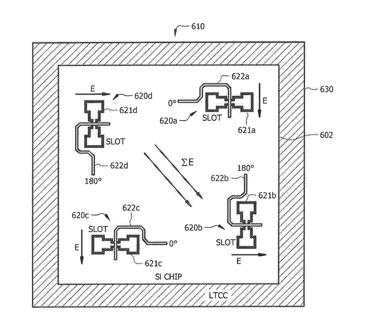
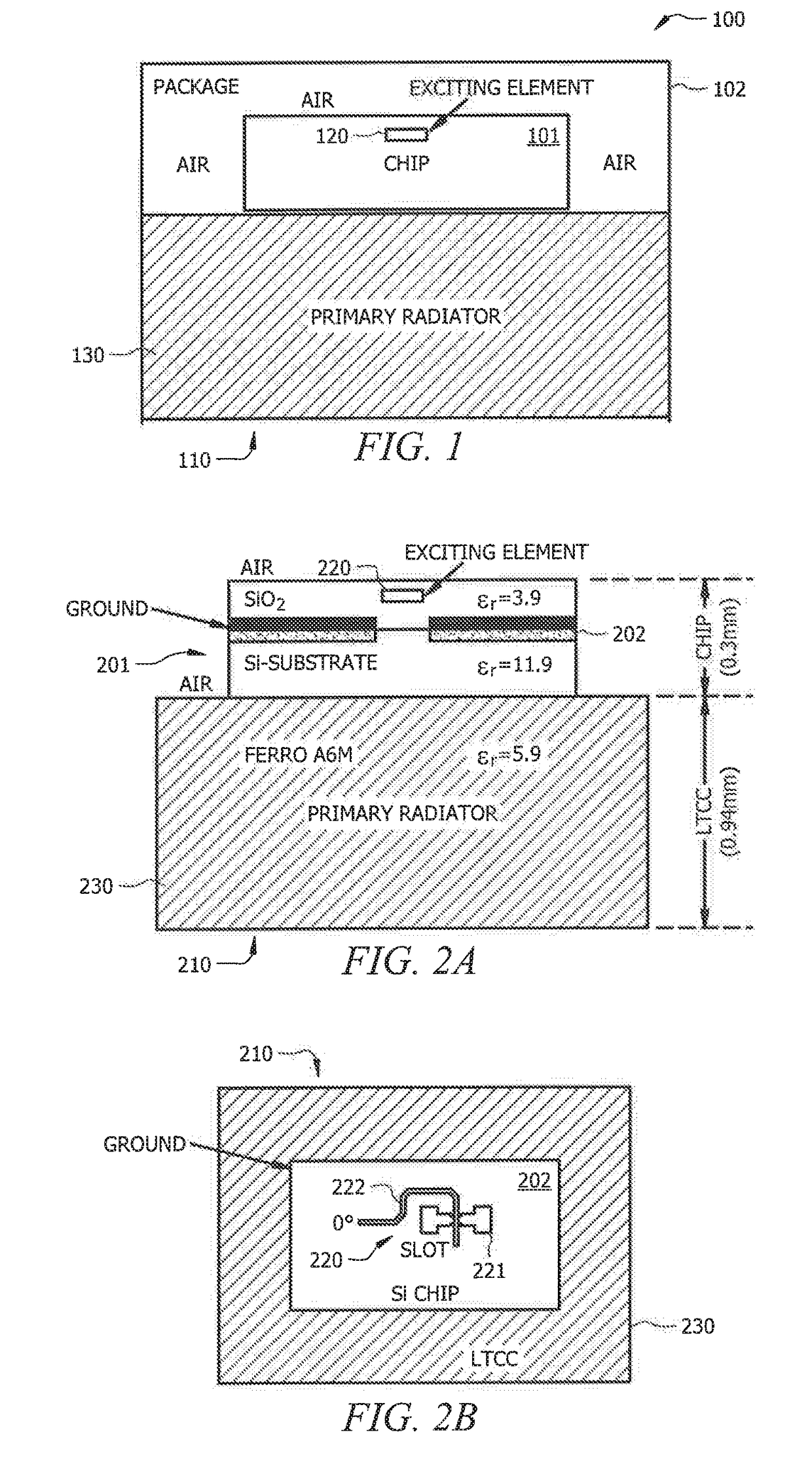
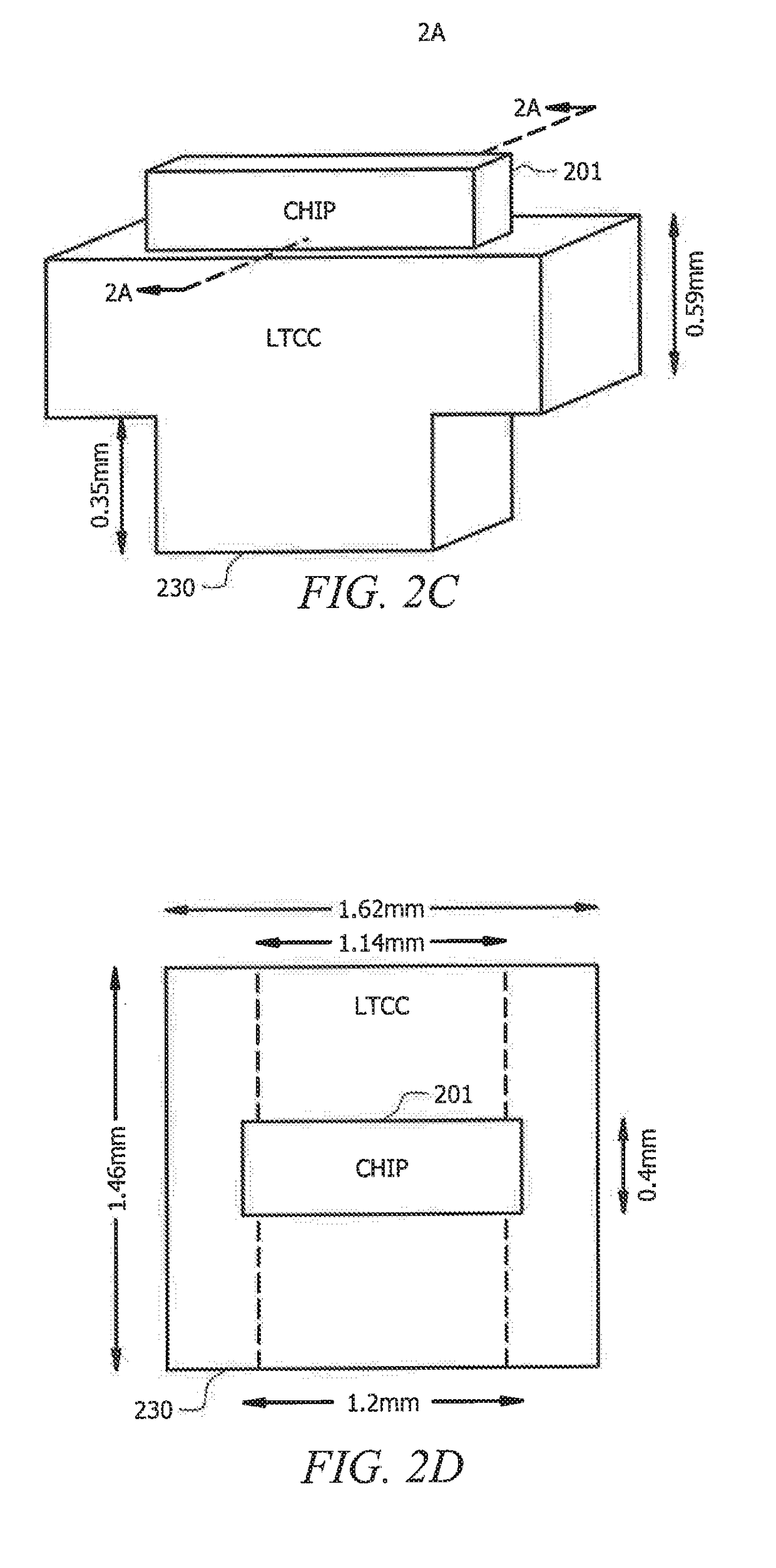
[0021]FIG. 1 shows a cross section view of integrated circuit product 100 configured according to the concepts of the present invention. Integrated circuit product 100 of the illustrated embodiment comprises chip 101 disposed in package 102. Chip 101 of embodiments comprises an integrated circuit die (e.g., dielectric substrate), such as may have various circuit components (e.g., transistors, resistors, capacitors, inductors, transmission lines, etc.) of a radiator and / or receiver system disposed therein. Package 102 of embodiments provides a protective housing in which chip 101 is disposed and through which one or more pins or other input-output interfaces may be provided. Accordingly, integrated circuit product 100 may provide a RF system module (e.g., integrated circuit component) or RF system (e.g., SOC or SIP) implementation, such as may be utilized in high speed wireless communications systems, imaging systems, spectroscopy systems, sensor systems, etc.

[0022]Integrated circuit...


PUM


Abstract

Systems and methods which provide an antenna in a chip-and-package distributed configuration as disclosed. Chip-and-package distributed antenna configurations of embodiments comprise an on-chip integrated circuit component and an in-package component. For example, embodiments of a chip-and-package distributed antenna comprise an exciting element on chip (i.e., formed as an integrated component in an integrated circuit die) and a primary radiator in package (i.e., disposed within an package while being external to the integrated circuit die). The on-chip exciting element may be configured to excite electromagnetic waves and to provide relatively wide bandwidth operation while occupying a relatively small area of the die. The in-package primary radiator may be configured to leverage the relatively large space in the integrated circuit product package to enhance the gain and/or configure the radiation pattern of RF signals with respect to the exciting element.

Description

TECHNICAL FIELD[0001]The invention relates generally to antennas for radiating and receiving signals and, more particularly, to chip-and-package distributed antenna configurations.BACKGROUND OF THE INVENTION[0002]The use of radio frequency (RF) signals, such as for providing wireless communication of voice, images, and data, for use in imaging, to provide sensing, etc., is commonplace to the point of nearly becoming ubiquitous. Due to various reasons, such as the availability of relatively unused spectrum, radiation providing penetration of a wide variety of materials, etc., the use of RF signals at higher and higher frequencies has become of interest. For example, the terahertz (THz) band from 0.3 THz to 3 THz is gaining increasing interest due to its potential for use with respect to various applications, such as imaging, spectroscopy, and high-speed wireless communication.[0003]An antenna is an indispensable component of any RF radiating system to radiate out the signal generated...

Claims


Application Information

Patent Timeline
Patent Type & Authority Applications(United States)
IPC IPC(8): H01Q1/22H01Q1/36H01Q13/10H01Q21/06
CPCH01Q1/2283H01Q21/064H01Q13/10H01Q1/36
Inventor XUE, QUANWU, LIANGLIAO, SHAOWEI
Owner CITY UNIVERSITY OF HONG KONG
Why Eureka
Try Eureka