
Finfet thyristors for protecting high-speed communication interfaces

a high-speed communication and finfet technology, applied in the direction of diodes, electronic switching, pulse techniques, etc., can solve the problems of electronic system design constraints to safely handle these types of environmental overstress conditions, electrical overstress events, electrical signals, etc., to achieve the effect of preventing electrical overstress events

Active Publication Date: 2021-11-04
ANALOG DEVICES INC
View PDF3 Cites 1 Cited by
  • Summary
  • Abstract
  • Description
  • Claims
  • Application Information

AI Technical Summary

Benefits of technology

The patent describes a new type of semiconductor device called Fin field-effect transistor (FinFET) thyristors that can protect high-speed communication interfaces from damage caused by overcurrent or high radio frequency power. These thyristors offer high voltage tolerance, low capacitance, and wide bandwidth operation, making them ideal for providing electrical overstress protection for FinFET-based integrated circuits. The FinFET thyristors also have a triggering circuit that improves their turn-on speed and reduces resistance during the on state.

Problems solved by technology

Electronic systems can be exposed to electrical overstress events, or electrical signals of short duration having rapidly changing voltage and high power during manufacturing, assembly, and end-user application environment.
The electronic systems design constraints to safely handle these type of environmental overstress conditions is more complex in fin field-effect-transistor (FinFET) systems-on-a-chip (SoC) for high frequency and high data rate applications.
Electrical overstress events can damage or destroy integrated circuits (ICs) by generating overvoltage conditions and high levels of power dissipation in relatively small areas of the ICs.
High power dissipation can increase IC temperature, and can lead to numerous problems, such as gate oxide punch-through, junction damage, metal damage, and surface charge accumulation.

Method used


Image

  • Finfet thyristors for protecting high-speed communication interfaces
  • Finfet thyristors for protecting high-speed communication interfaces
  • Finfet thyristors for protecting high-speed communication interfaces

Examples


Embodiment Construction

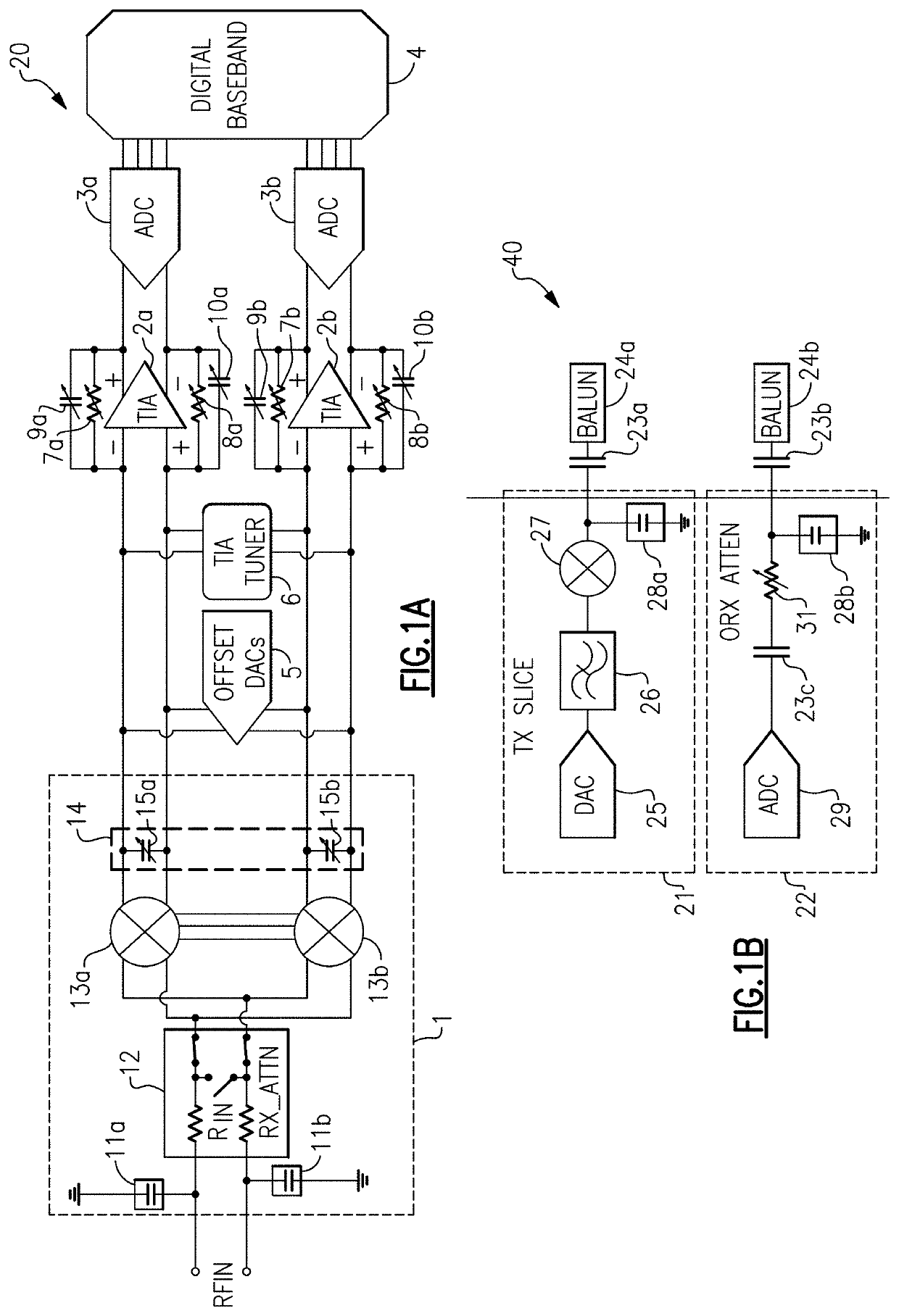
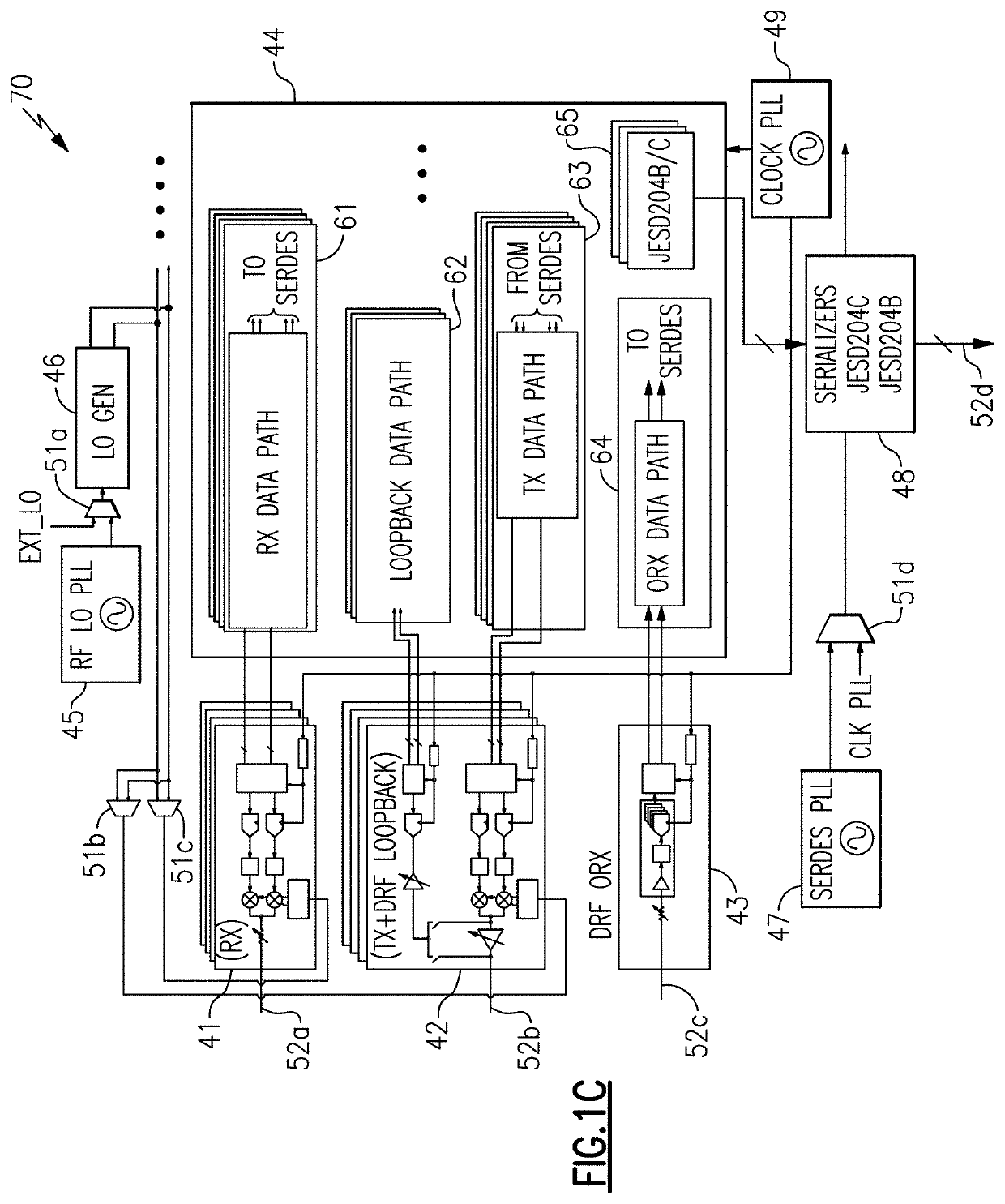
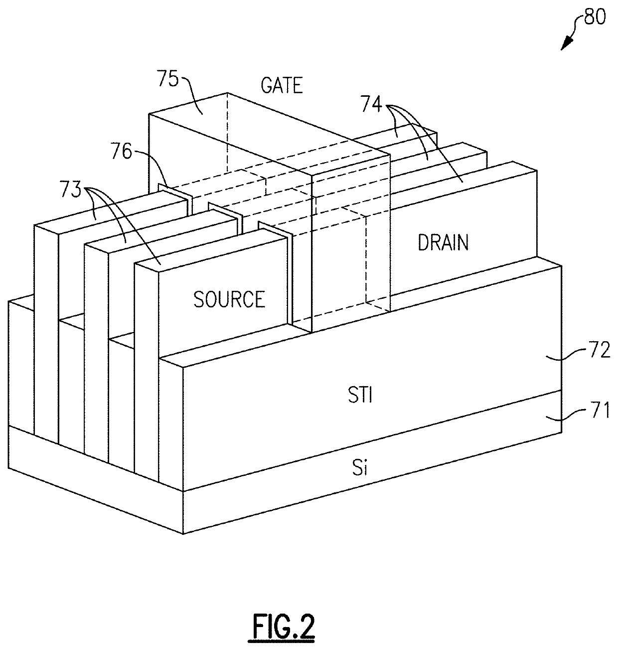
[0076]The following detailed description of embodiments presents various descriptions of specific embodiments of the invention. However, the invention can be embodied in a multitude of different ways in fin field-effect-transistor (FinFET) technology. In this description, reference is made to the drawings where like reference numerals may indicate identical or functionally similar elements. It will be understood that elements illustrated in the figures are not necessarily drawn to scale. Moreover, it will be understood that certain embodiments can include more elements than illustrated in a drawing and / or a subset of the elements illustrated in a drawing. Further, some embodiments can incorporate any suitable combination of features from two or more drawings.

[0077]Certain electronic systems include overstress protection circuits to protect circuits or components from electrical overstress events. To help guarantee that an electronic system is reliable, manufacturers can test the ele...


PUM


Abstract

Fin field-effect transistor (FinFET) thyristors for protecting high-speed communication interfaces are provided. In certain embodiments herein, high voltage tolerant FinFET thyristors are provided for handling high stress current and high RF power handling capability while providing low capacitance to allow wide bandwidth operation. Thus, the FinFET thyristors can be used to provide electrical overstress protection for ICs fabricated using FinFET technologies, while addressing tight radio frequency design window and robustness. In certain implementations, the FinFET thyristors include a first thyristor, a FinFET triggering circuitry and a second thyristor that serves to provide bidirectional blocking voltage and overstress protection. The FinFET triggering circuitry also enhances turn-on speed of the thyristor and / or reduces total on-state resistance.

Description

FIELD OF THE DISCLOSURE[0001]Embodiments of the invention relate to electronic systems with radio frequency high data rate communication interfaces, and more particularly to, electrical overstress protection for such systems.BACKGROUND[0002]Electronic systems can be exposed to electrical overstress events, or electrical signals of short duration having rapidly changing voltage and high power during manufacturing, assembly, and end-user application environment. Electrical overstress events include, for example, electrical overstress (EOS), electromagnetic interference (EMI), and electrostatic discharge (ESD) arising from the abrupt release of charge from an object or person to an electronic system. The electronic systems design constraints to safely handle these type of environmental overstress conditions is more complex in fin field-effect-transistor (FinFET) systems-on-a-chip (SoC) for high frequency and high data rate applications.[0003]Electrical overstress events can damage or d...

Claims


Application Information

Patent Timeline
Patent Type & Authority Applications(United States)
IPC IPC(8): H03K17/081H01L29/74H01L29/78H01L27/02
CPCH03K17/08108H01L27/0262H01L29/785H01L29/742H01L29/7412H01L29/7436H01L29/0657
Inventor SALCEDO, JAVIER A.PFEIFER, JONATHAN G.
Owner ANALOG DEVICES INC
Learn More