

Display device
a technology of display device and display screen, which is applied in the direction of semiconductor devices, electrical appliances, basic electric elements, etc., can solve the problems of short life, low brightness, and current leakage through a continuous organic film, and achieve the effect of smaller non-light-emitting region and higher aperture ratio
- Summary
- Abstract
- Description
- Claims
- Application Information
AI Technical Summary
Benefits of technology
Problems solved by technology
Method used
Image

Examples
first embodiment
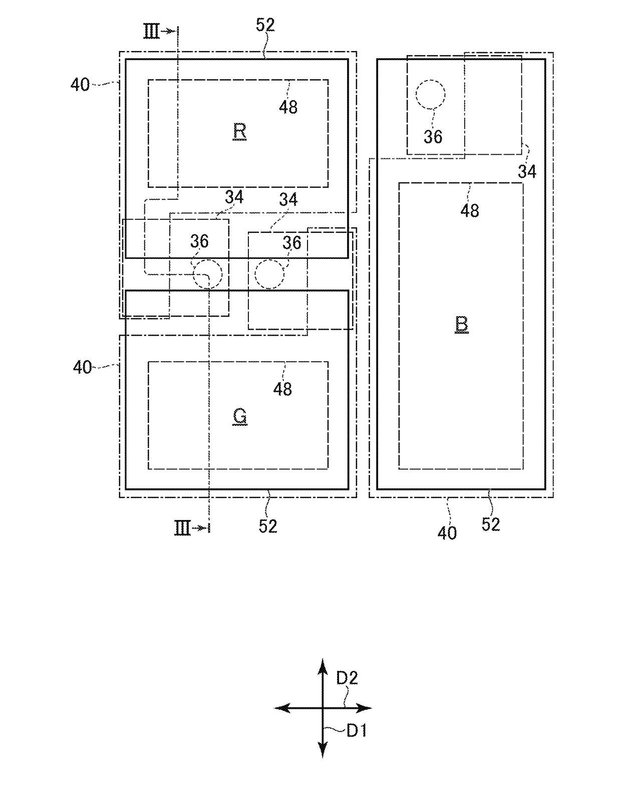
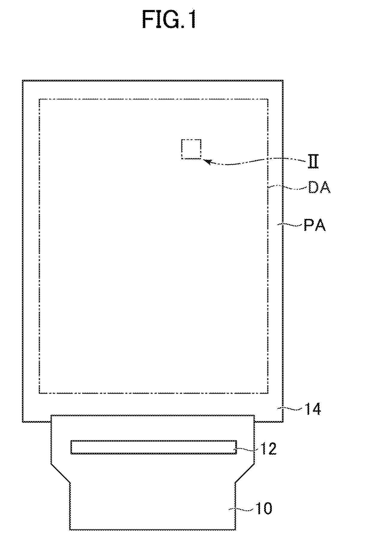
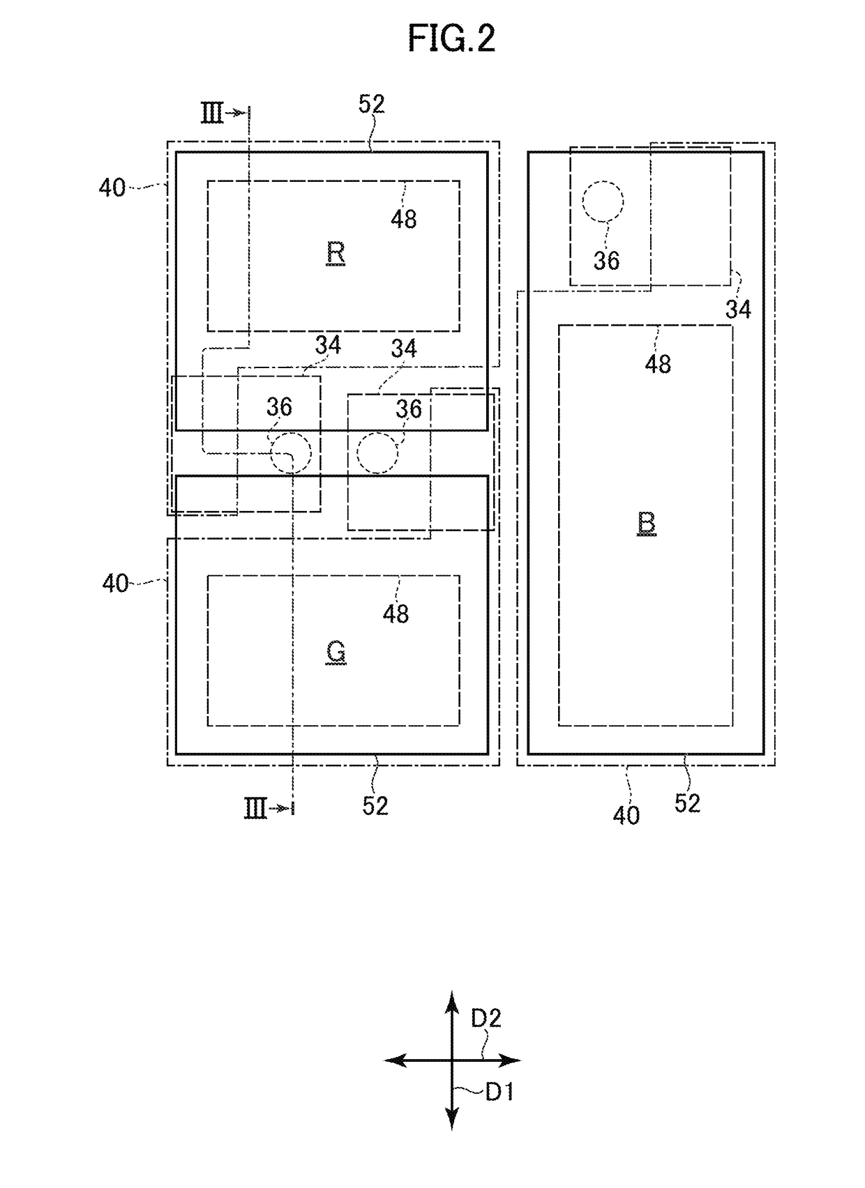
[0024]FIG. 1 is a plan view of a display device in accordance with a first embodiment. The display device is an organic electroluminescence display device. The display device is configured to display a full-color image in full-color pixels, each of which consists of combination of unit pixels (subpixels) of colors such as red, green, and blue. The display device includes a display area DA on a substrate 14 and a peripheral area PA around the display area DA. The peripheral area PA is outside the display area DA. A flexible printed circuit board 10 is connected to the peripheral area PA on the substrate 14. On the flexible printed circuit board 10 is mounted an integrated circuit chip 12 for driving elements to display the image. The integrated circuit chip 12 may be alternatively mounted on the substrate 14.
[0025]FIG. 2 is an enlarged view of a portion of II-II line cross section of the display device in FIG. 1. In this example, the full color pixel consists of a red subpixel R, a g...
second embodiment
[0043]FIG. 4 is an enlarged plan view of a portion of a display device in accordance with a second embodiment. FIG. 5 is an enlarged view of V-V line cross section of the display device in FIG. 4. In this embodiment the organic electroluminescence layer 254 has a low conductive portion 272 with lower conductivity than other portions. The low conductive portion 272 is between an adjacent pair of pixel electrodes 252 among the plurality of pixel electrodes 252. The low conductive portion 272 continuously surrounds at least a central portion of each of the plurality of pixel electrodes 252.
[0044]The plurality of pixel electrodes 252 fall into some groups for respective colors. The light emitting layer 258 is configured to emit light of a corresponding one of the colors in the groups. The details are explained in the first embodiment. The low conductive portion 272 is between an adjacent pair of pixel electrodes 252 in different groups. The light emitting layer 258, between the adjacent...
third embodiment
[0049]FIG. 6 is a cross sectional view of a display device in accordance with a third embodiment. This embodiment is different from the second embodiment in FIG. 5 in that the pixel electrode 352 includes a light reflective layer 344A.
[0050]The light reflective layer 344A is on an opening edge 350 without overlapping with an opening 348 of an insulation layer 346. The pixel electrode 352 further includes a transparent conductive layer 342 made from material such as indium tin oxide (ITO). The light reflective layer 344A is under the transparent conductive layer 342; a light emitting element 364 generates light, which passes through the transparent conductive layer 342 and is reflected on the light reflective layer 344A over the insulation layer 346, reducing attenuation of the light because of its reflection without passaging through the insulation layer 346. The transparent conductive layer 342 is connected to the underlying electrode 340 in the opening 348. The underlying electrod...
PUM
 Abstract
Description
Claims
Application Information