Routable electroforming substrate comprising removable carrier

a technology of electroforming substrate and removable carrier, which is applied in the direction of semiconductor/solid-state device details, semiconductor devices, electrical apparatus, etc., can solve the problems of warpage or cracks in the substrate, impose limitations on the ability to make semiconductor packages even thinner, and reduce yield and cost. , to achieve the effect of more robust handling

Active Publication Date: 2018-10-25
ADVANCED ASSEMBLY MATERIALS INTERNATIONAL LIMITED
View PDF3 Cites 7 Cited by
  • Summary
  • Abstract
  • Description
  • Claims
  • Application Information

AI Technical Summary

Benefits of technology

[0006]It is thus an object of the invention to seek to provide a substrate used for semiconductor assembly and package that is suitable for assembling thin packages and are inherently more robust during handling in the semiconductor assembling process.

Problems solved by technology

A problem with the said approach is that, for very thin package substrates, such as those which are 100 μm or thinner, many challenges such as warpage or cracks in the substrate are encountered during the manufacturing of the substrate, as well as during its handling in the semiconductor assembly process.
These lead to lower yield and higher costs, and impose limitations on the ability to make the semiconductor packages even thinner.

Method used


Image

  • Routable electroforming substrate comprising removable carrier
  • Routable electroforming substrate comprising removable carrier
  • Routable electroforming substrate comprising removable carrier

Examples


Embodiment Construction

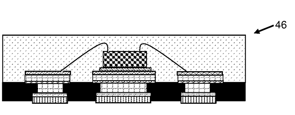
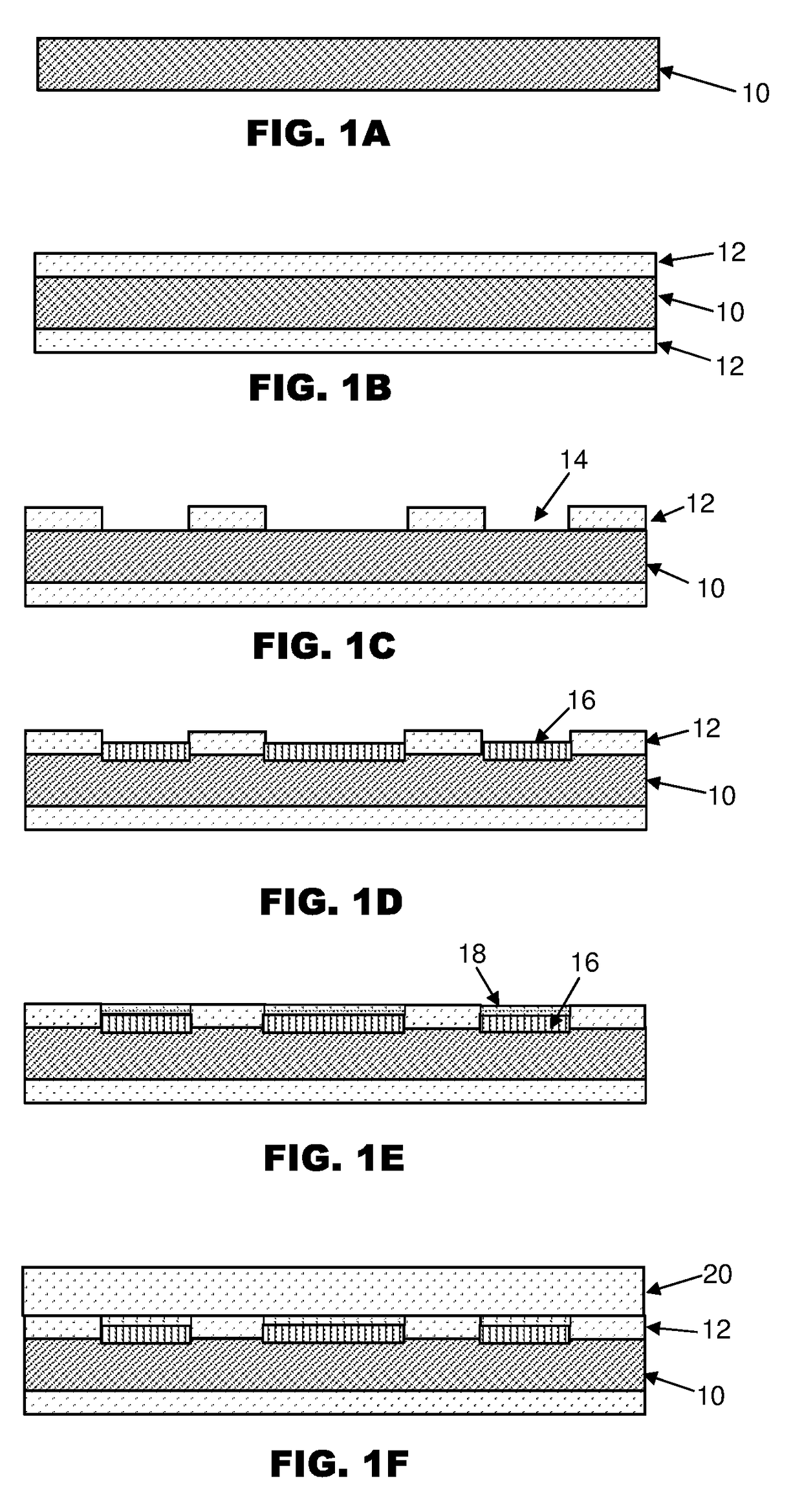
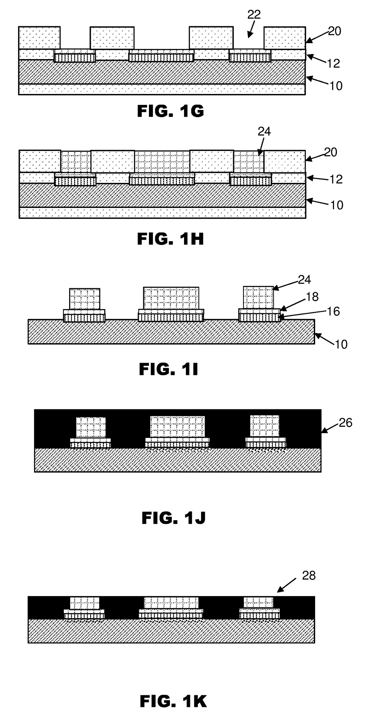
[0014]FIGS. 1A to 1P illustrate a process for fabricating a routable electroforming substrate for assembling a semiconductor package according to the preferred embodiment of the invention. In FIG. 1A, a substrate carrier 10 is provided. The substrate carrier 10 is made of an electrically conductive material and is preferably attractable by magnetic forces. In one embodiment, the substrate carrier 10 comprises stainless steel, in particular stainless steel grade 430. The surfaces of the substrate carrier 10 should first be chemically treated to remove all stains, oil marks and contamination prior to usage to ensure that they are clean.

[0015]In FIG. 1B, first photo-resist layers 12 are formed onto the surfaces of the substrate carrier 10, by laminating and covering top and bottom surfaces of the substrate carrier 10 with photosensitive dry film. In FIG. 1C, the first photo-resist layer 12 is patterned by selective exposure of the first photo-resist layer 12 to ultraviolet light, or by...


PUM


Abstract

A routable electroforming substrate for assembling a semiconductor package is manufactured by providing a carrier and plating a patterned first metallic layer onto the carrier which is configured to function as a surface mount pad or input / output pad in an assembled semiconductor package. A patterned second metallic layer comprising copper is plated over the first metallic layer, and a third metallic layer, which is configured for mounting a plurality of semiconductor dice, is plated over the second metallic layer. The carrier is then removed to expose the first metallic layer.

Description

FIELD OF THE INVENTION[0001]The invention relates to substrates used in the assembly and packaging of electronic devices.BACKGROUND AND PRIOR ART[0002]Conventionally, semiconductor packages have been manufactured from assembling semiconductor dice on substrates in the form of lead frames. Such substrates support the semiconductor dice during die bonding, wire bonding and encapsulation of the dice and wire bonds. After encapsulation, the substrates and encapsulant are cut or singulated to form separate semiconductor packages.[0003]Driven by portable devices, wearable devices and other consumer products, there is an increasing demand in the semiconductor packaging industry to produce devices with smaller form factors. To do so, thinner substrates which are more compact and have routable circuits are required to attain the objects of such cost-effective advanced packaging solutions.[0004]For instance, U.S. Pat. No. 7,795,071 entitled “Semiconductor Package for Fine Pitch Miniaturizatio...

Claims


Application Information

Patent Timeline
Patent Type & Authority Applications(United States)
IPC IPC(8): H01L21/48H01L21/56H01L23/00H01L23/31H01L23/498
CPCH01L21/4857H01L21/56H01L24/85H01L24/49H01L23/3121H01L23/49822H01L23/14H01L23/31H01L2224/32225H01L2224/48229H01L2224/73265H01L2224/83192H01L2224/83855H01L21/568H01L2221/68345H01L2224/2919H01L2924/181H01L24/45H01L2224/45144H01L2224/45147H01L21/486H01L23/49827H01L2924/00014H01L2924/0665H01L2924/00012
Inventor CHAN, TAT CHIKWAN, YIU FAIVILLAESPIN, GIO JOSE ASUMOLAM, YU LUNGREN, HANG
Owner ADVANCED ASSEMBLY MATERIALS INTERNATIONAL LIMITED
Why Eureka
Try Eureka