Die-bonding substrate, high-density integrated cob white light source and method for manufacturing the same

a technology of white light source and integrated cob, which is applied in the field can solve the problems of affecting the light quality and operation stability of white light source, the power of a single chip is unable to meet the requirements of illumination field, and the essential drawback of low luminous flux of white light led, etc., to achieve high luminous efficiency, increase effective light output, and high luminous flux

Active Publication Date: 2018-11-01
FUJIAN CAS CERAMIC OPTOELECTRONICS TECH CO LTD
View PDF2 Cites 0 Cited by
  • Summary
  • Abstract
  • Description
  • Claims
  • Application Information

AI Technical Summary

Benefits of technology

[0034]The advantageous effects of the present invention are as follows:
[0035]1. Through an optimized configuration of the array chips on the die-bonding substrate and an optimized layout and division of the conductive line layer, the drainage of heat flow of the chips that emitting light and heat is guaranteed, the uniformity of the radiation lights excited by the chips is ensured, and a high-density integration and a high-power encapsulation of the light source is realized.
[0036]2. Through the arrangement of the reflective dam body, and the optimization of the wire bonding process, the effective light output is increased. The encapsulated light source is characterized by a high luminous flux, a high luminous efficiency and a low cost.
[0037]3. By improving the wire-welding manner, the present invention reduces the distance of the heat conduction from the fluorescent ceramic sheet to the heat dissipation system, thereby reducing the temperature of the fluorescent ceramic and improving its reliability and luminous efficiency.

Problems solved by technology

The poor thermally conducting performance of fluorescent gel, and the directly contacting with the excitation chips that emitting light and heat, easily lead to thermal aging of the coated fluorescent powder gel, which affects the light quality and operation stability of the white light source.
In terms of illumination popularization and application, the white-light LED still has an essential drawback of low luminous flux.
Obviously, the power of a single chip is unable to meet the requirements of the illumination field on high brightness and high power.

Method used


Image

  • Die-bonding substrate, high-density integrated cob white light source and method for manufacturing the same
  • Die-bonding substrate, high-density integrated cob white light source and method for manufacturing the same
  • Die-bonding substrate, high-density integrated cob white light source and method for manufacturing the same

Examples


Embodiment Construction

[0045]In order to make the objective, the technical solutions and the advantage of the present invention more intelligible, the present invention will be described in greater detail in combination with the embodiments with reference to the accompanying drawings. It is to be understood by those skilled in the art that the present invention is not limited to the drawings and the following embodiments.

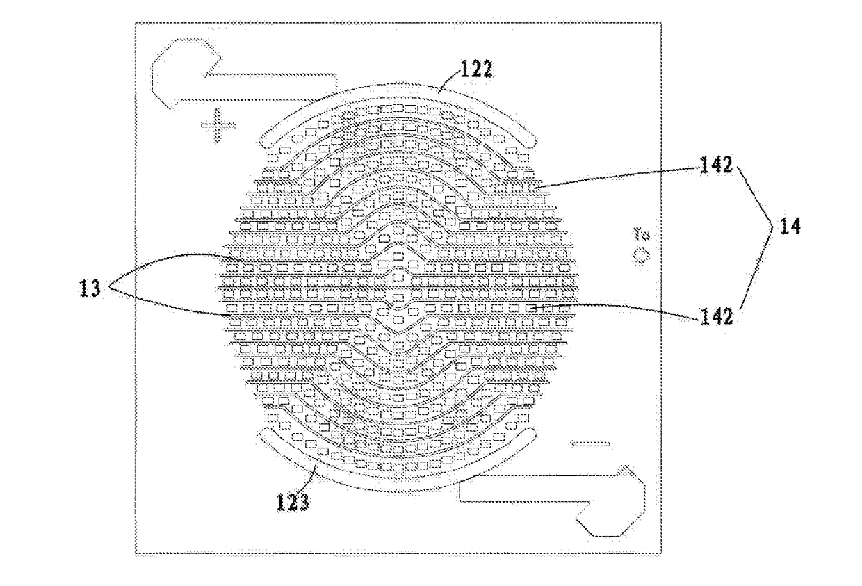
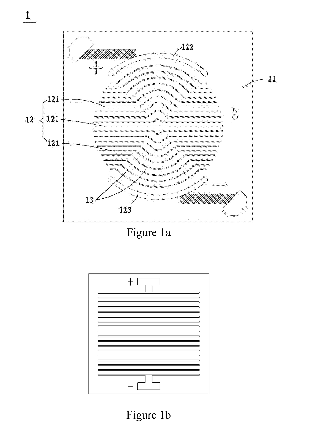
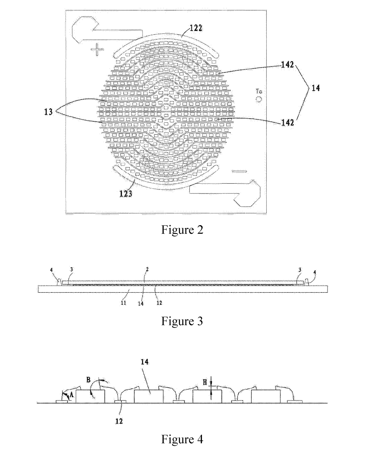
[0046]As shown in FIGS. 1 to 4, the high-density integrated COB white light source according to the present invention includes a die-bonding substrate 1 and a solid-state phosphor 2, and it further includes height-limiting retainers 3 and a reflective dam body 4. The solid-state phosphor 2 is located right ahead of the die-bonding substrate 1, the height-limiting retainers 3 are provided on the die-bonding substrate 1 for supporting the solid-state phosphor 2, and they are 150-350 microns higher than the die-bonding substrate 1. The reflective dam body 4 is made of a highly reflecting col...


PUM


Abstract

A die-bonding substrate has a substrate, and a conductive line layer and a chip array provided on the substrate. The conductive line layer includes a chip welding wire region and an external electrode region connected with each other. The chip welding wire region is composed of multiple conductive lines, wherein the central conductive line located in the central position of the chip welding wire region is a straight line section. The conductive lines arranged at both sides of the central conductive line are straight line sections at both ends, and arc sections curved outwards in the middle, so that the entire chip welding wire region forms a circular area. The array chips are arranged inside the circular area, and are electrically connected with the conductive lines arranged at both sides. The entire chip welding wire region can also form a rectangular area.

Description

TECHNICAL FIELD[0001]The present invention relates to a white light source, in particular to a die-bonding substrate, a high-density integrated COB white light source, and a method for manufacturing the same.BACKGROUND ART[0002]By virtue of the high efficiency and the power-saving performance, LED illumination exhibits economic benefits, such as notable consumption reduction, energy saving, etc., and therefore has been vigorously promoted and widely applied in many illumination fields and other industries in recent years. At the current level of industrial technology, the technique of LED monochromatic chip added with phosphor is still the dominant fashion to achieve a white-light LED. The most common encapsulation form is excitation chips coated with fluorescent powder gel. The poor thermally conducting performance of fluorescent gel, and the directly contacting with the excitation chips that emitting light and heat, easily lead to thermal aging of the coated fluorescent powder gel...

Claims


Application Information

Patent Timeline
Patent Type & Authority Applications(United States)
IPC IPC(8): H01L25/075H01L33/62H01L33/50H01L33/60H01L33/64H01L33/56
CPCH01L25/0753H01L33/62H01L33/505H01L33/60H01L33/647H01L33/56H01L2933/0066H01L2933/005H01L33/48H01L2933/0058H01L2933/0075H01L2224/4809H01L2933/0091H01L25/075H01L33/005H01L33/483H01L33/52H01L33/54
Inventor YE, SHANGHUIZHANG, JIEQINHONG, MAOCHUNLIN, WENXIONGGUO, WANGZHANG, YUNFENG
Owner FUJIAN CAS CERAMIC OPTOELECTRONICS TECH CO LTD
Why Eureka
Try Eureka