

Semiconductor device and method for forming the same
a technology of semiconductor devices and membranes, applied in the direction of semiconductor devices, basic electric elements, electrical equipment, etc., can solve the problems of parasitic electron accumulation, memory cells leaking their charges, and troublesome problems existing in dram devices regarding buried word line structures,
- Summary
- Abstract
- Description
- Claims
- Application Information
AI Technical Summary
Benefits of technology
Problems solved by technology
Method used
Image

Examples
Embodiment Construction
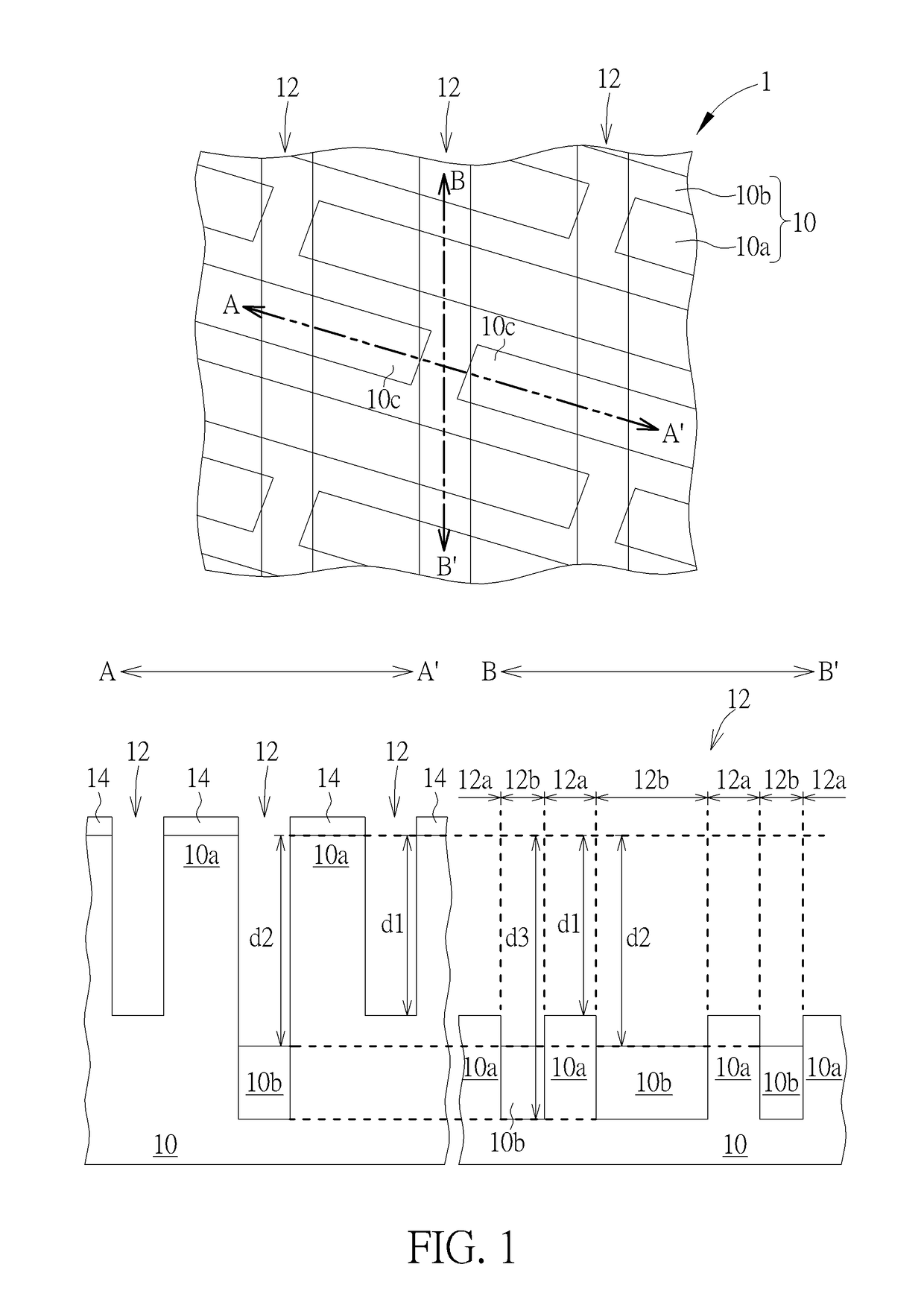
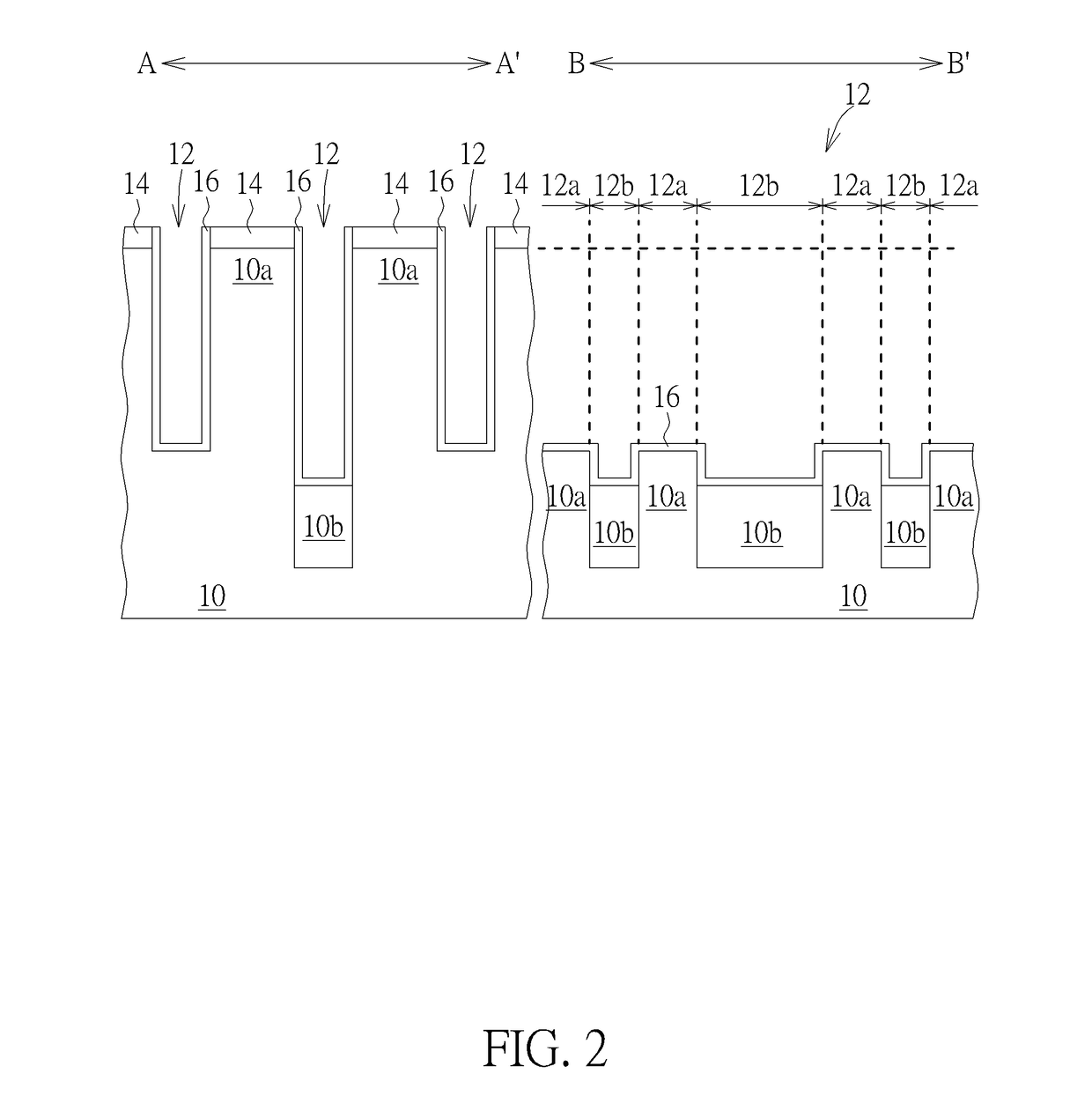
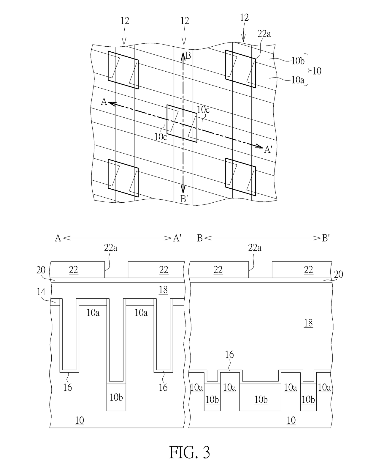
[0015]FIG. 1 to FIG. 9 are schematic diagrams illustrating the process of forming a semiconductor structure according to a preferred embodiment of the present invention. The semiconductor structure 1 in the preferred embodiment may be a dynamic random access memory (DRAM) device having buried word lines. In FIGS. 1, 3, 4 and 7, the upper portions are top views of the semiconductor structure 1 in different process steps. The lower-left portions and lower-right portions are cross-sectional views taken along line A-A′ and line B-B′ in the top views. It is noteworthy that line A-A′ and line B-B′ intersect at a region between adjacent terminals 10c of active regions 10a along line A-A′, which is substantially the passing gate (PG) region of a buried word line formed in the gate trench 12 along line B-B. For the sake of simplicity, FIGS. 2, 5, 6, 8 and 9 only shows cross-sectional views taken along line A-A′ and line B-B′. In the following description, the extending direction of line B-B′...
PUM
 Abstract
Description
Claims
Application Information