Fine metal mask and manufacture method thereof

Inactive Publication Date: 2018-12-13
WUHAN CHINA STAR OPTOELECTRONICS TECH CO LTD
View PDF2 Cites 11 Cited by
  • Summary
  • Abstract
  • Description
  • Claims
  • Application Information

AI Technical Summary

Benefits of technology

[0006]An objective of the present invention is to provide a fine metal mask, which can provide the pixel openings with a smaller size and can be us

Problems solved by technology

Generally, the resolution of conventional FMMs is difficult to be applied for manufacturing the display devices with a resolution greater than 250 ppi.
With

Method used


Image

  • Fine metal mask and manufacture method thereof
  • Fine metal mask and manufacture method thereof
  • Fine metal mask and manufacture method thereof

Examples


Example

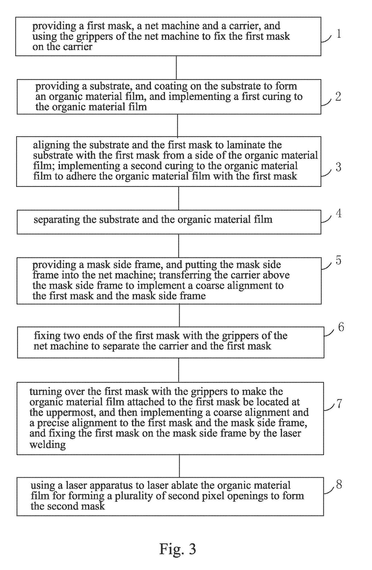
[0079]For better explaining the technical solution and the effect of the present invention, the present invention will be further described in detail with the accompanying drawings and the specific embodiments.

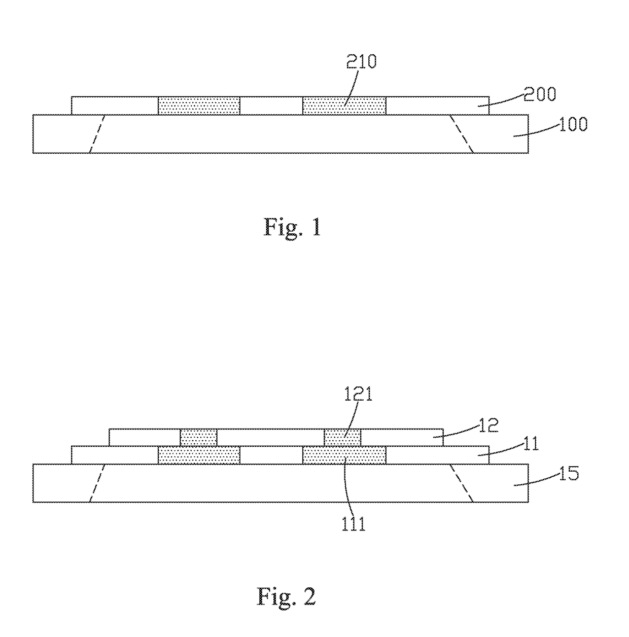
[0080]Please refer to FIG. 2. The present invention provides a fine metal mask, comprising a mask side frame 15, a first mask 11 fixed on the mask side frame 15 and a second mask 12 located on the first mask 11;

[0081]the first mask 11 comprising a plurality of first pixel openings 111;

[0082]the second mask 12 comprising one or more second pixel openings 121 corresponding to an area of each first pixel opening 111;

[0083]the first mask 11 being a metal mask, and the second mask 12 being an organic material mask.

[0084]Specifically, a material of the second mask 12 is polyimide or polyamide, and a thickness of the second mask 12 is smaller than 50 μm, and preferably is 20 μm or thinner, and the second pixel openings 121 thereon can be formed by a method of laser ablation.

[0085]Spe...


PUM

PropertyMeasurementUnit
Thicknessaaaaaaaaaa
Thicknessaaaaaaaaaa
Forceaaaaaaaaaa

Abstract

The present invention provides a fine metal mask and a manufacture method thereof. The fine metal mask comprises a mask side frame, a first mask of metal material and a second mask of an organic material; the first mask comprising first pixel openings; the second mask comprising one or more second pixel openings corresponding to an area of each first pixel opening, and because the second pixel openings are arranged in the area corresponding to the first pixel openings, in comparison with prior art, the present invention can provide the pixel openings with a smaller size to manufacture the OLED elements with a smaller size to raise the resolution of the OLED display product; meanwhile, the opening wall slope of the second pixel openings can be controlled to be smaller to make the incident angle of the evaporation material at the second pixel opening edge smaller.

Description

FIELD OF THE INVENTION[0001]The present invention relates to a manufacture field of an Organic Light Emitting Diode, and more particularly to a fine metal mask and a manufacture method thereof.BACKGROUND OF THE INVENTION[0002]Organic Light Emitting Diode (OLED) is a flat panel display technology which has great prospects for development. It possesses extremely excellent display performance, and particularly the properties of self-illumination, simple structure, ultra thin, fast response speed, wide view angle, low power consumption and capability of realizing flexible display, and therefore is considered as the “dream display”. Meanwhile, the investment for the production equipments is far smaller than the TFT-LCD. It has been favored by respective big display makers and has become the main selection of the third generation display element of the display technology field. At present, the OLED has reached the point before mass production. With the further research and development, th...

Claims


Application Information

Patent Timeline
IPC IPC(8): C23C14/04C23C14/24
CPCC23C14/042C23C14/24H01L27/3211H01L51/56C23C14/0005C23C14/12H10K71/166H10K71/00H10K59/35
Inventor MU, JUNYING
Owner WUHAN CHINA STAR OPTOELECTRONICS TECH CO LTD
Why Eureka
Try Eureka