
Organic electroluminescent device

a technology of electroluminescent display device and organic electroluminescent light, which is applied in the direction of basic electric elements, semiconductor devices, electrical apparatus, etc., can solve the problems of increasing production cost, increasing production cost, and increasing the thickness of the screen body

Active Publication Date: 2018-12-13
KUNSHAN NEW FLAT PANEL DISPLAY TECH CENT
View PDF0 Cites 3 Cited by
  • Summary
  • Abstract
  • Description
  • Claims
  • Application Information

AI Technical Summary

Benefits of technology

The present invention provides an organic electroluminescent device that utilizes a special material called a TADF material in the green light units of the device. This material helps to decrease the concentration of triplet excitons and prevents them from diffusing to the blue light layer, resulting in a green light spectrum that does not contain any blue light components. Additionally, the device does not require a hole-blocking layer, simplifying the structure and reducing production costs.

Problems solved by technology

In this technology, each subpixel is a structurally-complete organic light-emitting diode, two many stacked layers in a single pixel unit add to the control difficulty during the preparation process, and because each diode is individually driven by a respective driving circuit, the corresponding pixel circuit is complicated, which also adds to the process difficulty, and as a result, the reliability of the organic electroluminescent display device is prone to decline.
The color filter method needs to add a layer of color filter upon the light-exiting surface of a white organic light-emitting diode, which not only increases the production cost but also increases the thickness of the screen body.
More importantly, the color filter will considerably absorb the light emitted from the OLED device and thus severely reduce the external quantum efficiency of the OLED device.
In the primary pixel collocation method, each pixel is formed by an arrangement of 2-4 primary subpixels, and during manufacturing, a fine metal mask is required for preparing each subpixel, at least three deposition or transfer steps are required, with very high requirements of process precision, and as a result, in actual production, mixing of different primary colors usually occurs, which causes a problem that negatively affects the display quality.
Meanwhile, in prior art, in order to prevent the problem of phosphorescent material aggregation quenching, the light-emitting layer is usually prepared by doping a host material with a guest material, which leads to a problem that holes move faster than electrons, therefore, a hole-blocking layer with adapted energy level must be provided on one side of the light-emitting layer away from the anode, so as to ensure the carriers with opposite electrical properties recombine within the light-emitting layer, which further adds to the process difficulty.
However, in order to ensure the light spectrums emitted from the red and green subpixels do not contain a blue light component, there usually is a limitation to the energy level of the light-emitting material.
In this literature, the HOMO energy level of the blue light material is limited to be not lower than 5.5 eV, which considerably limits the selection range of the blue light material.

Method used


Image

  • Organic electroluminescent device
  • Organic electroluminescent device
  • Organic electroluminescent device

Examples


embodiment 1

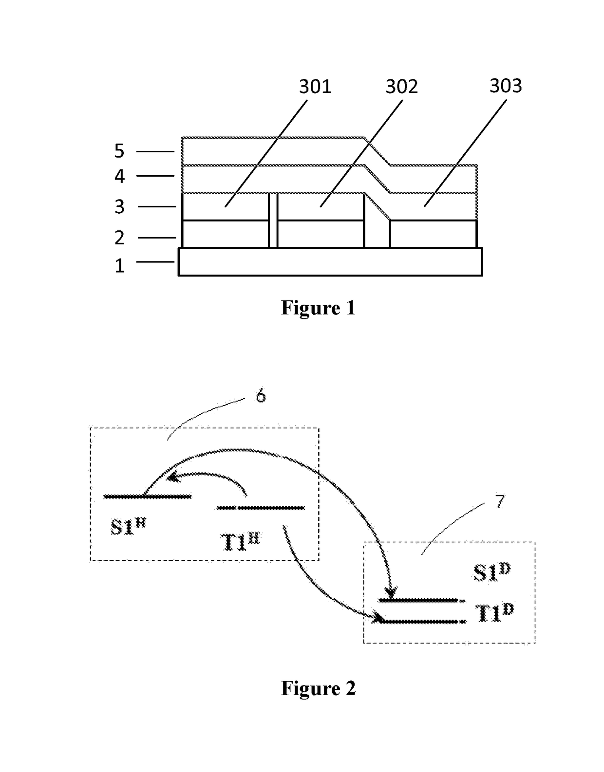
[0027]This embodiment provides an organic electroluminescent device, as shown in FIG. 1, comprising a first electrode 2, a first light-emitting layer 3, a second light-emitting layer 4 and a second electrode 5 stacked upon a substrate 1, wherein the first light-emitting layer 3 comprises red light units 301, green light units 302 and blue light units 303, which are arranged in the same layer, and the second light-emitting layer 4 is a blue light layer. In this embodiment, preferably, the blue light unit 303 in the first light-emitting layer 3 is formed by a part of the second light-emitting layer 4 extending into the first light-emitting layer 3, that is to say, the blue light unit 303 has the same material as that of the second light-emitting layer 4.

[0028]As an alternative embodiment of the present invention, the material of the blue light unit 303 may also be different from that of the second light-emitting layer 4, which can also achieve the purpose of the present invention and ...

embodiment 2

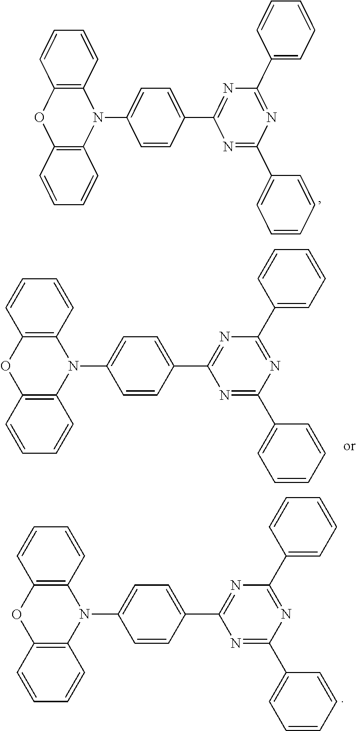
[0034]This embodiment provides an organic electroluminescent device with the same device structure as that of Embodiment 1, and the difference is that the host material of the red light unit 301 is the Thermal Activation Delayed Fluorescence material of formula (1-1) and the host material of the green light unit 302 is the Thermal Activation Delayed Fluorescence material of formula (1-2).

embodiment 3

[0035]This embodiment provides an organic electroluminescent device with the same device structure as that of Embodiment 1, and the difference is that the host material of the green light unit 302 is the Thermal Activation Delayed Fluorescence material of formula (1-11).


PUM


Abstract

An organic electroluminescent device adopts a TADF material as a first host material (6) of a green light unit (302) to sensitize a green phosphorescent material serving as a first guest material (7). A portion of triplet excitons are converted into singlet excitons through inverse gap crossing, and thus decrease of the triplet exciton concentration results in narrowing of the recombination region, thereby preventing the triplet excitons from diffusing into a blue light layer (4) to emit light, so as to realize a green light spectrum containing no blue light component. And because an energy level difference between red light and blue light is relatively large, carriers in a red light unit cannot be easily transferred to the blue light layer, and therefore it is not easy for a blue light component to appear in a red light spectrum. Accordingly, the light-emitting spectrums of red / green subpixels in the organic electroluminescent device with a shared blue light layer do not contain blue light, thereby effectively broaden the range of applicable combinations of luminescent materials and improving the display performance of the device. Moreover, a hole-blocking layer is not required, and thus the structure of the device is effectively simplified, and the operation voltage is lowered; in the meantime, the process difficulty is reduced, and the product yield is increased, thereby reducing the production cost.

Description

TECHNICAL FIELD[0001]The present invention relates to the field of organic electroluminescence, and in particular relates to an organic electroluminescent device and a preparation method thereof.BACKGROUND[0002]Organic Light-Emitting Devices (OLED) adopts organic electroluminescent material and is a type of active light-emitting device, with the advantages of low power consumption, wide color gamut and thinner volume, and has the prospect of becoming the next-generation mainstream illuminance and flat panel display technology.[0003]Currently, the organic electroluminescent display technology has been widely used in small-sized panels such as smart phone display screens. At present, the main techniques for an organic electroluminescent display device to realize full-color display are in the following three ways: the first way is primary pixel collocation method, such as P (Pentile) collocation and IGNIS collocation (see Chinese patent CN102714213A); the second way is using color filt...

Claims


Application Information

Patent Timeline
Patent Type & Authority Applications(United States)
IPC IPC(8): H01L27/32H01L51/50
CPCH01L27/3211H01L51/504H01L51/5016H01L51/5084H01L51/5056H10K85/654H10K50/121H10K50/11H10K2101/10H10K59/35H10K50/13H10K2101/20H10K59/00H10K50/00H10K50/15H10K50/167
Inventor SONG, GAOSONG, LIUFEI, ZHAO
Owner KUNSHAN NEW FLAT PANEL DISPLAY TECH CENT
Learn More