Voltage-switched magneto-resistive random access memory (MRAM) employing separate read operation circuit paths from a shared spin torque write operation circuit path

Active Publication Date: 2019-01-03
QUALCOMM INC
View PDF2 Cites 27 Cited by
  • Summary
  • Abstract
  • Description
  • Claims
  • Application Information

AI Technical Summary

Benefits of technology

[0010]Aspects disclosed in the detailed description include voltage-switched magneto-resistive random access memory (MRAM) employing separate read operation circuit paths from a shared spin torque write operation circuit path. In exemplary aspects disclosed herein, the MRAM includes an MRAM array that includes one or more MRAM bit cell rows that each include a plurality of MRAM bit cells. Each MRAM bit cell includes a magnetic tunnel junction (MTJ) device that is configured to either be in a parallel (P) or anti-parallel (AP) magnetization state to store representations of a logical ‘0’ and ‘1’ for providing memory storage. MRAM bit cells on an MRAM bit cell row share a common electrode (e.g., top or bottom electrode) to provide a shared write operation circuit path. Two write operation transistors coupled to each end portion of the common electrode are activated in response to a write operation to form a write circuit path for write current to flow between the write operation transistors. The write operation transistors are controlled to control direction of the write current through the common electrode, which controls the direction of spin torque applied to the respective MTJ device of the MTJ bit cells. To write data to selected MRAM bit cells in the MRAM bit cell row, a negative voltage is applied to each non-shared electrode of the MRAM bit cells to be written to lower the energy barrier of its respective MTJ device with the spin torque applied as

Problems solved by technology

Read parasitic resistance affects the tunnel magnetoresistance

Method used


Image

  • Voltage-switched magneto-resistive random access memory (MRAM) employing separate read operation circuit paths from a shared spin torque write operation circuit path
  • Voltage-switched magneto-resistive random access memory (MRAM) employing separate read operation circuit paths from a shared spin torque write operation circuit path
  • Voltage-switched magneto-resistive random access memory (MRAM) employing separate read operation circuit paths from a shared spin torque write operation circuit path

Examples


Embodiment Construction

[0035]With reference now to the drawing figures, several exemplary aspects of the present disclosure are described. The word “exemplary” is used herein to mean “serving as an example, instance, or illustration.” Any aspect described herein as “exemplary” is not necessarily to be construed as preferred or advantageous over other aspects.

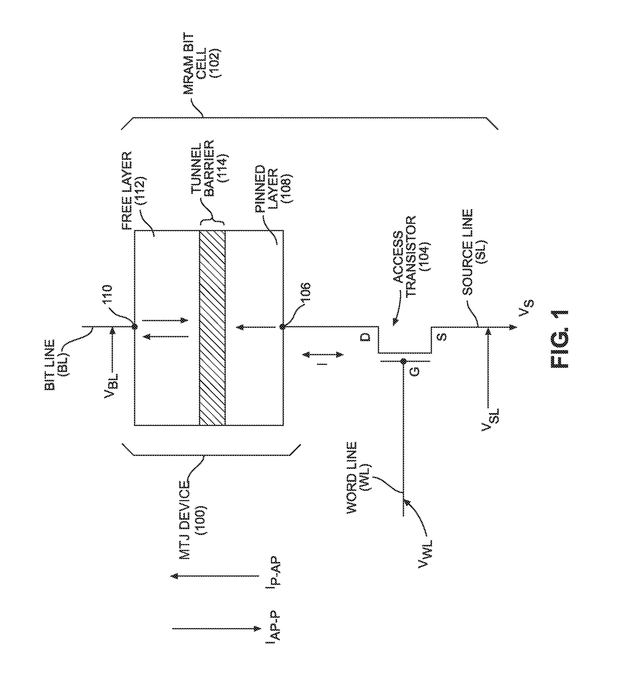
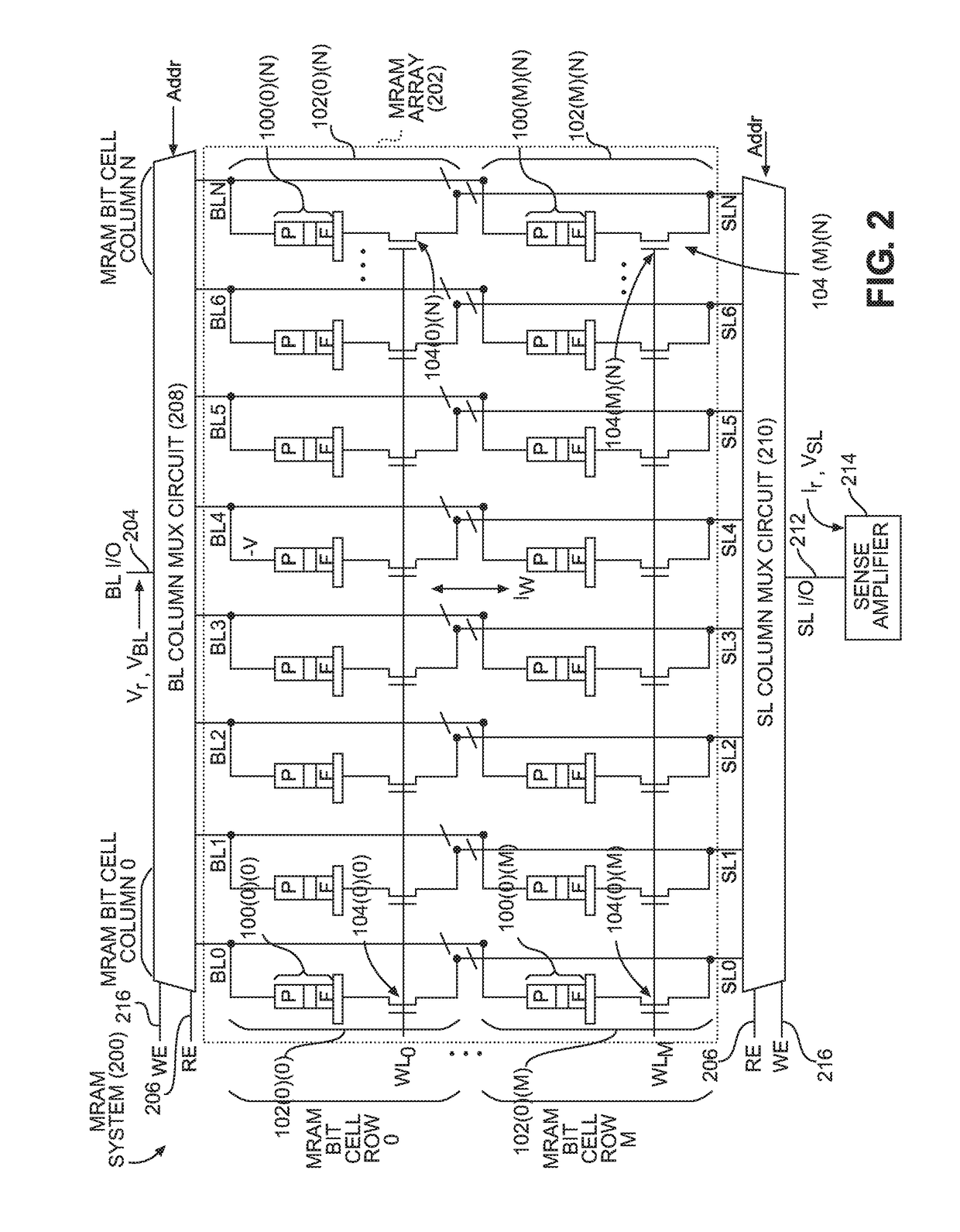
[0036]Aspects disclosed in the detailed description include voltage-switched magneto-resistive random access memory (MRAM) employing separate read operation circuit paths from a shared spin torque write operation circuit path. In exemplary aspects disclosed herein, the MRAM includes an MRAM array that includes one or more MRAM bit cell rows that each include a plurality of MRAM bit cells. Each MRAM bit cell includes a magnetic tunnel junction (MTJ) device that is configured to either be in a parallel (P) or anti-parallel (AP) magnetization state to store representations of a logical ‘0’ and ‘1’ for providing memory storage. MRAM bit cells on an MRAM b...


PUM


Abstract

Voltage-switched magneto-resistive random access memory (MRAM) employing separate read operation circuit paths from a shared spin torque write operation circuit path is disclosed. The MRAM includes an MRAM array that includes MRAM bit cell rows each including a plurality of MRAM bit cells. MRAM bit cells on an MRAM bit cell row share a common electrode to provide a shared write operation circuit path for write operations. Dedicated read operation circuit paths are also provided for each MRAM bit cell separate from the write operation circuit path. As a result, the read operation circuit paths for the MRAM bit cells do not vary as a result of the different layout locations of the MRAM bit cells with respect to the common electrode. Thus, the read parasitic resistances of the MRAM bit cells do not vary from each other because of their different coupling locations to the common electrode.

Description

BACKGROUNDI. Field of the Disclosure[0001]The technology of the disclosure relates generally to magneto-resistive random access memory (MRAM), and more particularly to MRAM employing spin torque magnetic tunnel junction (MTJ) devices in MRAM bit cells.II. Background[0002]Semiconductor storage devices are used in integrated circuits (ICs) in electronic devices to provide data storage. One example of a semiconductor storage device is magneto-resistive random access memory (MRAM). MRAM is non-volatile memory in which data is stored by programming a magnetic tunnel junction (MTJ) as part of an MRAM bit cell. One advantage of MRAM is that MTJs in MRAM bit cells can retain stored information even when power is turned off. This is because data is stored in the MTJ as a small magnetic element rather than as an electric charge or current.[0003]In this regard, an MTJ comprises a free ferromagnetic layer (“free layer”) disposed above or below a fixed or pinned ferromagnetic layer (“pinned laye...

Claims


Application Information

Patent Timeline
IPC IPC(8): H01L27/22H01L43/08H01L43/02G11C11/16
CPCH01L27/228G11C11/1655H01L43/02H01L43/08G11C11/1659G11C11/1673G11C11/1675H10B61/22H10N50/10H10N50/80
Inventor LI, XIAKAN, JIMMY JIANANKANG, SEUNG HYUKYANG, BINTAO, GENGMING
Owner QUALCOMM INC
Why Eureka
Try Eureka