Thin film transistor array substrate and preparing method therefor, and OLED display device

Active Publication Date: 2019-01-03
SHENZHEN CHINA STAR OPTOELECTRONICS SEMICON DISPLAY TECH CO LTD
View PDF9 Cites 5 Cited by
  • Summary
  • Abstract
  • Description
  • Claims
  • Application Information

AI Technical Summary

Benefits of technology

[0033]The thin film transistor array substrate provided in the embodiment of the present disclosure selects to use different semiconductor materials as the active layer for a driving transistor and a switching transistor that implement different functions in the thin film transistor array substrate. For the driving transistor that drives the light emitting diode, a metal oxide semiconductor material is adopted as the ac

Problems solved by technology

The active layer of the thin film transistor which uses a poly-silicon material has high mobility, but with a large leakage current and worse uniformity; while the active layer of the thin film transistor which uses the metal oxide semiconductor material has better uniformity, but with comparatively low mobility.
Therefore, in the thin film transistor array substrate of

Method used


Image

  • Thin film transistor array substrate and preparing method therefor, and OLED display device
  • Thin film transistor array substrate and preparing method therefor, and OLED display device
  • Thin film transistor array substrate and preparing method therefor, and OLED display device

Examples


Embodiment Construction

[0037]In order for the purpose, technical solution and advantages of the present disclosure to be clearer, specific implementations of the present disclosure will be explained below in details in conjunction with the figures. Examples of these preferred implementations are illustrated in the figures. The implementations of the present disclosure illustrated in the figures and described according to the figures are only exemplary, and the present disclosure is not limited to these implementations.

[0038]Here, it also needs to be explained that in order to prevent the present disclosure from being made unclear due to unnecessary details, the figures only illustrate structures and / or processing steps closely related to the solutions according to the present disclosure, and omit other details slightly related to the present disclosure.

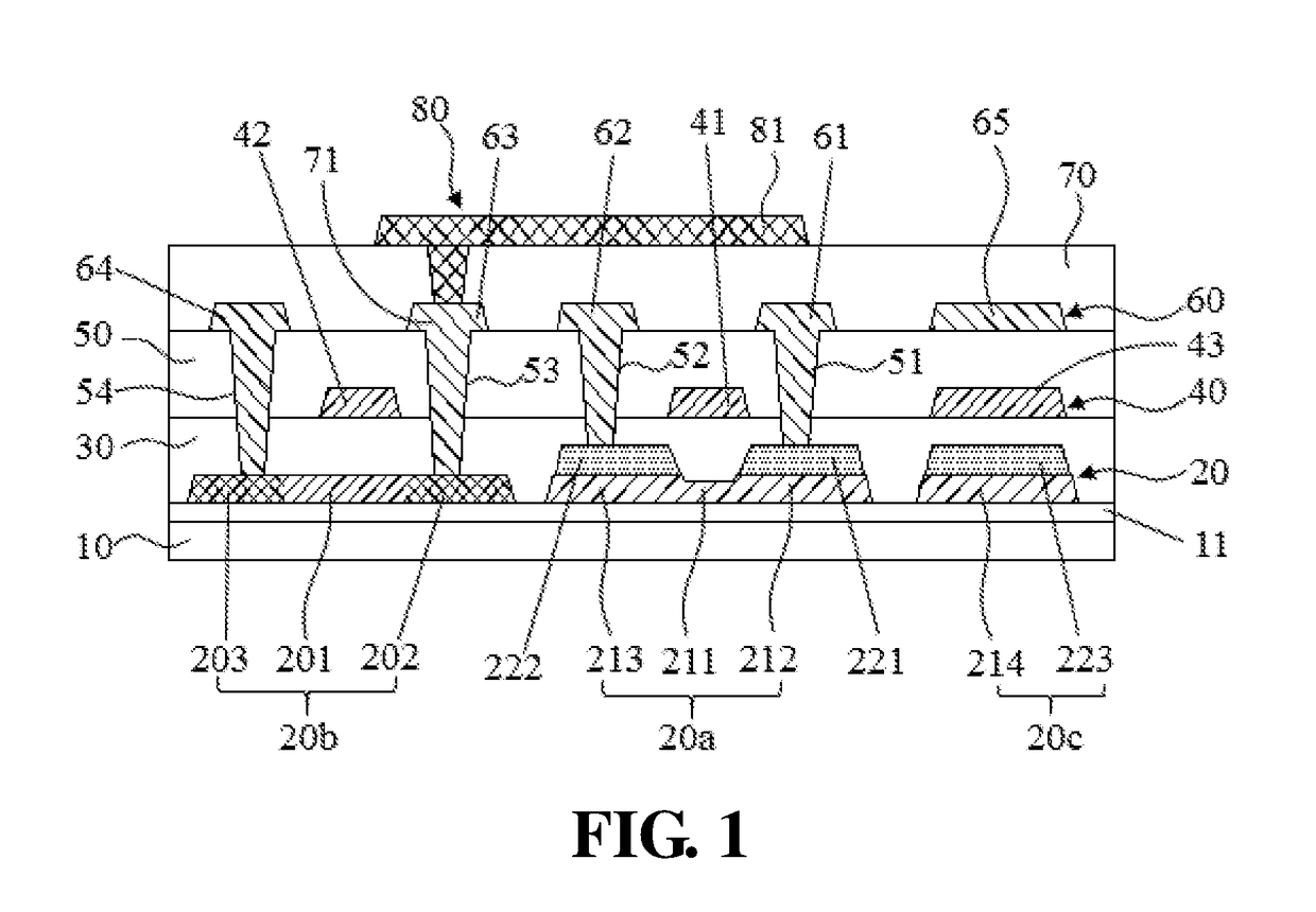
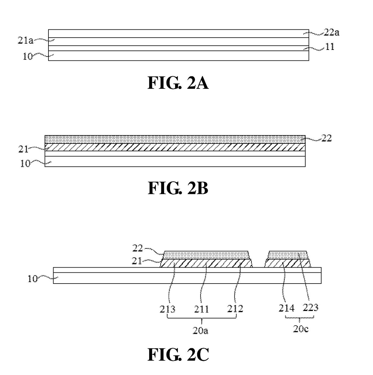
[0039]The present embodiment first provides a thin film transistor array substrate, as illustrated in FIG. 1, the thin film transistor array substrate incl...


PUM


Abstract

The present disclosure discloses a thin film transistor array substrate including an active layer disposed on a base substrate, wherein the active layer includes a first active region and a second active region located in a same structural layer, the first active region has a material comprising poly-silicon, and includes a first channel region, and a first source region and a first drain region that are located at both sides of the first channel region, respectively, the first source region having a first contact layer disposed thereon, the first drain region having a second contact layer disposed thereon, and materials of both the first and second contact layers being boron-doped poly-silicon; and the second active region has a material comprising metal oxide semiconductor, and includes a second channel region and a second source region and a second drain region that are located at both sides of the second channel region, respectively. The present disclosure also discloses a preparing method for the thin film transistor array substrate as mentioned above, and an OLED display device including the array substrate.

Description

TECHNICAL FILED[0001]The present disclosure relates to a display technical field, more particularly, to a thin film transistor array substrate and a preparing method therefor, and also relates to an OLED display device including the thin film transistor array substrate.BACKGROUND ART[0002]A flat panel display device has been widely applied for its many advantages such as a thin body, power saving, and radiation-free. Current flat panel display devices mainly include a Liquid Crystal Display (LCD), and an Organic Light Emitting Display (OLED). A Thin Film Transistor (TFT) is an important component of the flat panel display device, and may be formed on a glass substrate or a plastic substrate and is usually applied in for example LCD and OLED as a switching device and a driving device.[0003]At present, the OLED display device is a mainly current-controlled light emitting device, and the luminance uniformity is controlled by a corresponding current. Usually, a thin film transistor arra...

Claims


Application Information

Patent Timeline
IPC IPC(8): H01L27/32H01L27/12H01L29/49H01L29/417G09G3/3233
CPCH01L27/3262H01L27/3248H01L27/1255H01L27/3265H01L29/4908H01L29/41775G09G3/3233H01L27/1225H01L27/1229H10K59/123H10K59/1216H10K59/1213
Inventor ZHOU, XINGYU
Owner SHENZHEN CHINA STAR OPTOELECTRONICS SEMICON DISPLAY TECH CO LTD
Why Eureka
Try Eureka