Photoelectric Conversion Module

Active Publication Date: 2019-01-10
AQUAOPTICS CORP
View PDF5 Cites 10 Cited by
  • Summary
  • Abstract
  • Description
  • Claims
  • Application Information

AI Technical Summary

Benefits of technology

The invention proposes a photoelectric conversion module that includes an optical bench with at least one lens array and a circuit board with conductive trace formed thereon. The optical element is flip-chip connected to the circuit board with the lens array aligning to the beam bendable structure or the optical element. The module also includes an optical waveguide with a beam bendable structure. The at least one lens array may align to the beam bendable structure and the optical element, or to one end of the optical waveguide. The module may have an external optical element connected to the optical bench. The method for manufacturing the module involves combining the two optical benches. The technical effects of the invention are efficient coupling of optical elements to external optical elements and flexible components for optical waveguides.

Problems solved by technology

However, the active optical fiber connector can only be connected to the electronic device with electrical connection port, but not connected to the electronic device with optical connection port; and the passive optical fiber connector can only be connected to the electronic device with optical connection port, but not connected to the electronic device with electrical connection port.
Such packaging structure has the following disadvantages: (1) as the optical coupled element is fixed on the printed circuit board, it needs to consider the horizontal accuracy of packaging, but also needs to consider the vertical accuracy of the package; (2) optical signal within the optical coupled element with a longer optical path (about 2-3 mm), the optical field may be collimated in the internal of the optical coupled element by the lens, but the beam characteristics continues to diffuse.
However, fabrication of the micro lens needs to avoid the range of internal wires, which will limit the size of the micro lens, and thereby unfavorable to the design of the photo detector section.

Method used


Image

  • Photoelectric Conversion Module
  • Photoelectric Conversion Module
  • Photoelectric Conversion Module

Examples


Embodiment Construction

[0027]Some preferred embodiments of the present invention will now be described in greater detail. However, it should be recognized that the preferred embodiments of the present invention are provided for illustration rather than limiting the present invention. In addition, the present invention can be practiced in a wide range of other embodiments besides those explicitly described, and the scope of the present invention is not expressly limited except as specified in the accompanying claims.

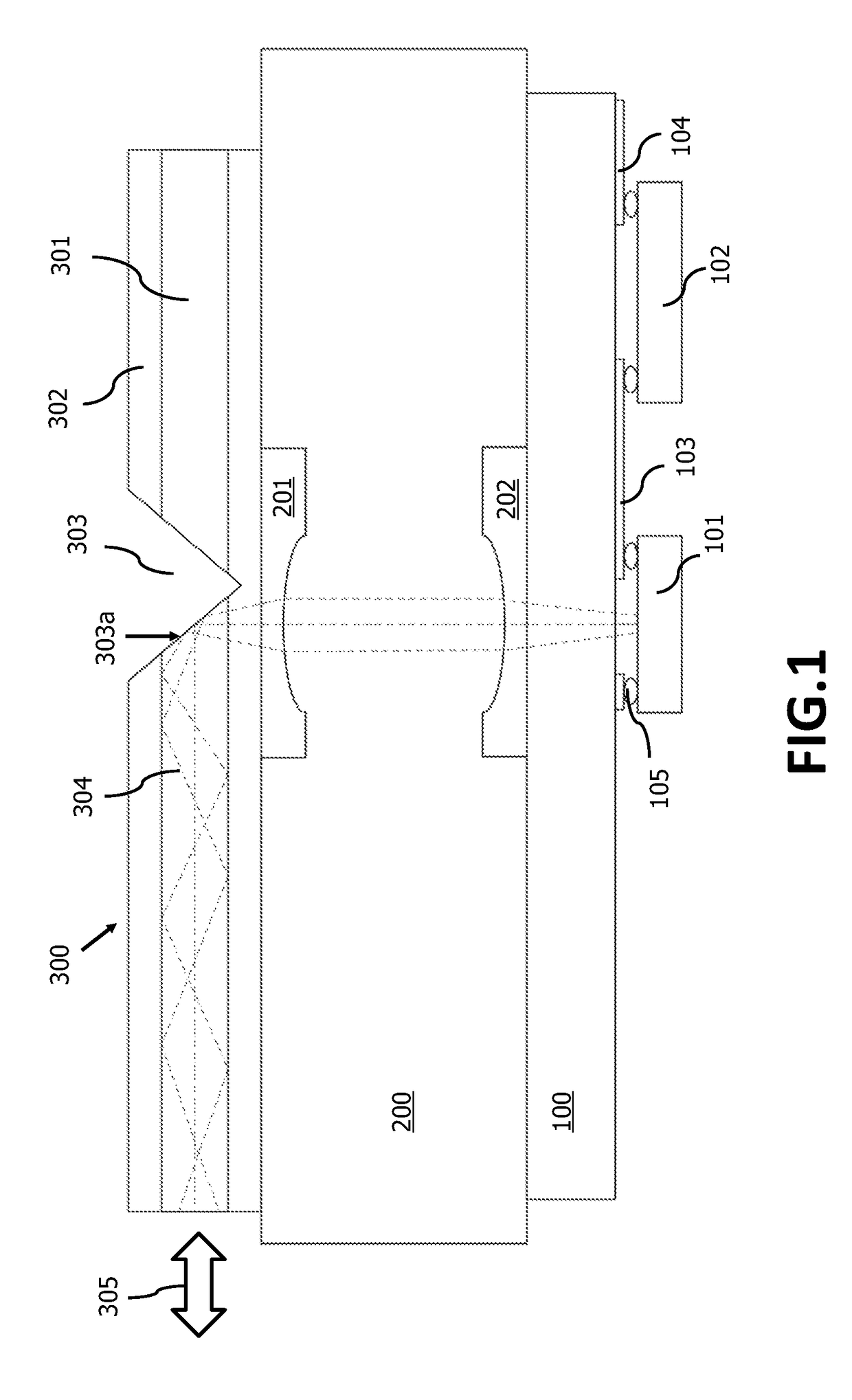
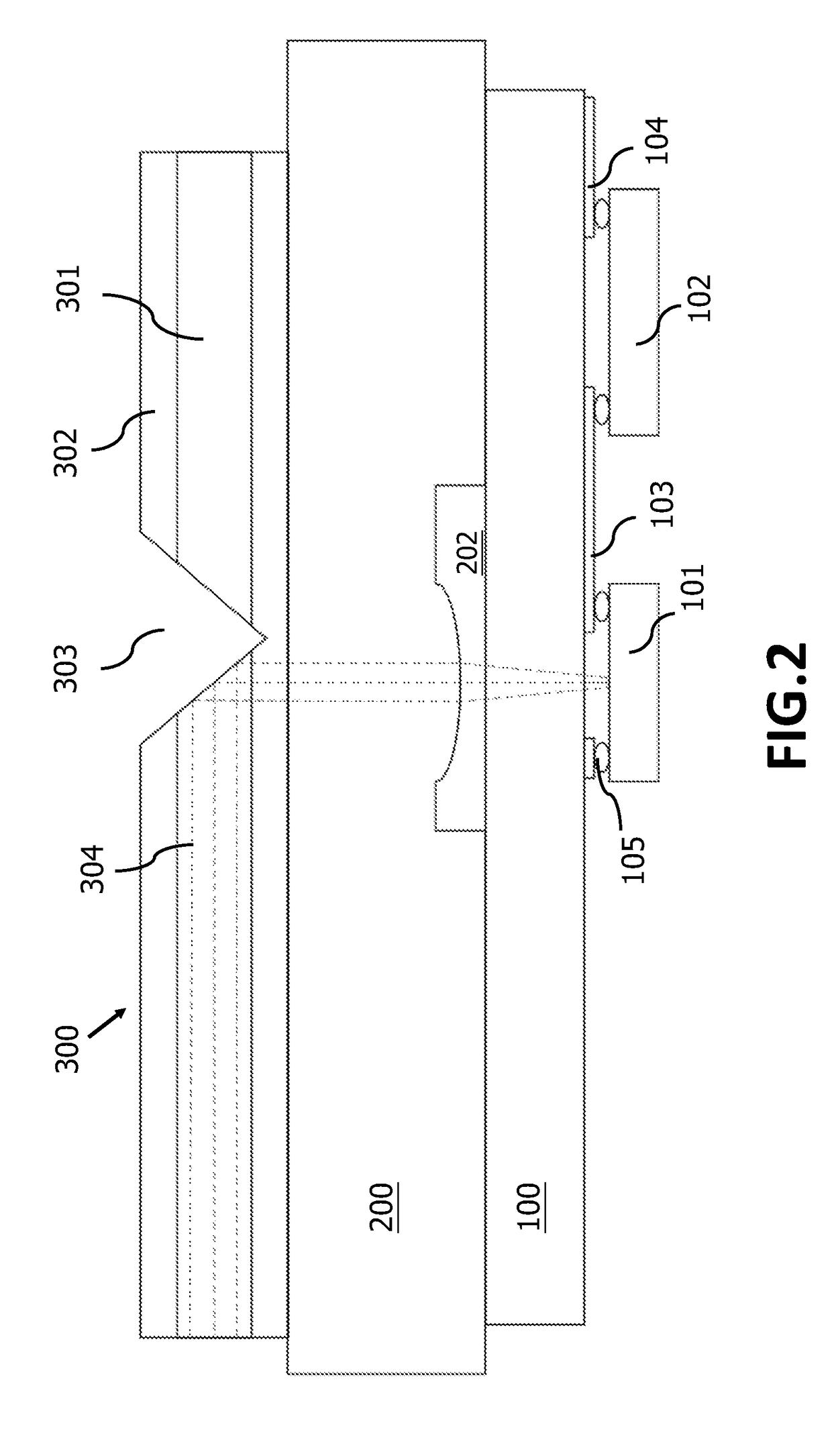
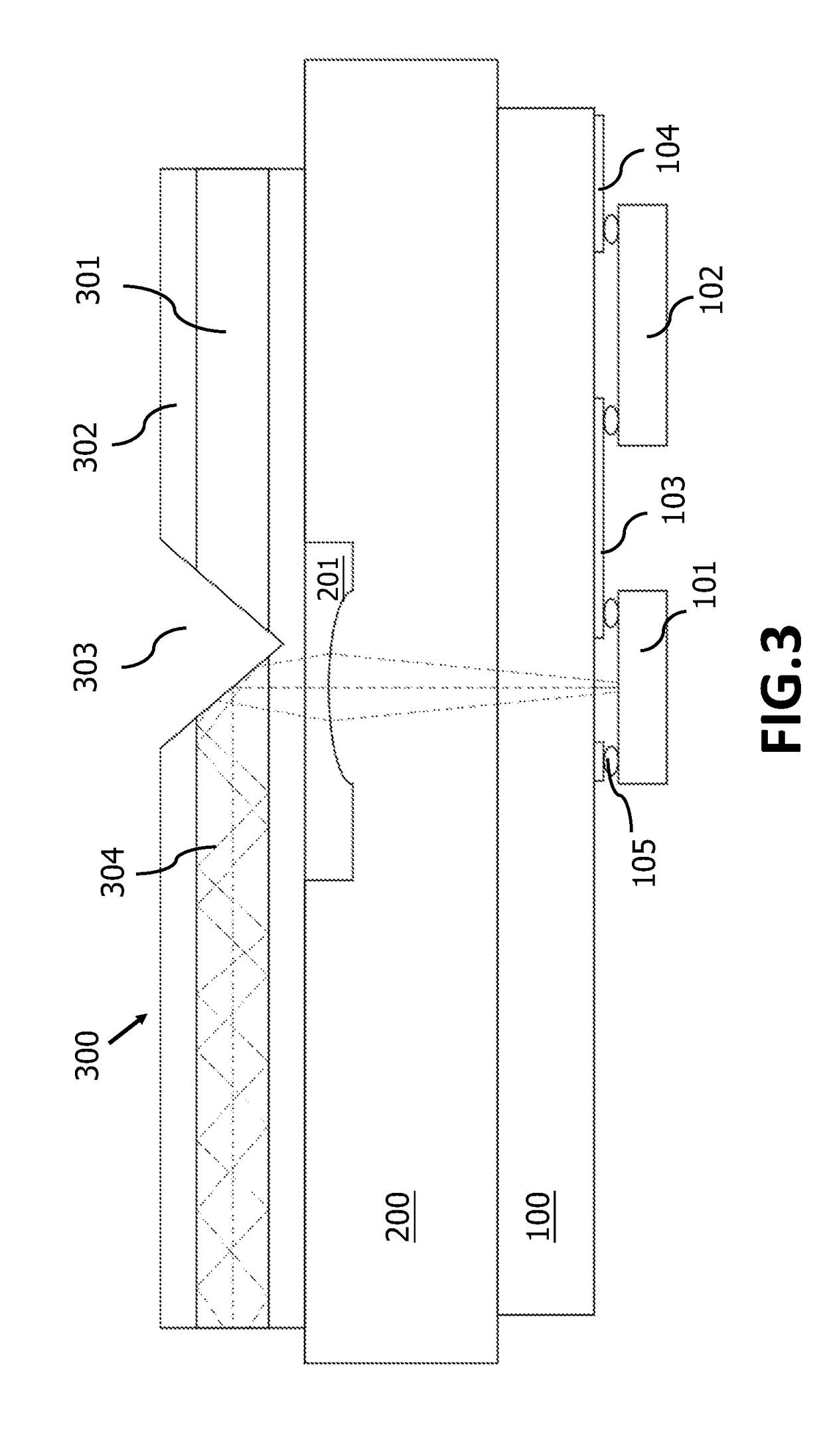
[0028]A photoelectric conversion module of the invention includes three portions:[0029](1) Optical waveguide: optical layer, the optical waveguide may be made of plastic material, which includes core portion and clad portion to construct the optical waveguide structure; in addition to the output and input of optical signals, the optical waveguide is also used for non-coplanar bending of the optical signals (via optical reflection surface of V-trench);[0030](2) Circuit board: electrical layer, p...


PUM


Abstract

A photoelectric conversion module comprises an optical bench having at least one lens array; a circuit board having conductive trace formed on the circuit board, configured on the optical bench; at least one optical element flip-chip packaged on the circuit board to couple to the conductive trace; and an optical waveguide having an optical reflection structure, wherein the at least one lens array aligns to the optical reflection structure or the at least one optical element.

Description

BACKGROUND OF THE INVENTIONField of the Invention[0001]The present invention relates to a photoelectric device, and more particularly, to a photoelectric conversion module which provides signal transmission and conversion between optical devices and electrical devices.Description of Related Art[0002]Light beams or optical signals are frequently used to transmit digital data between electronic devices, both over long distances and between adjacent circuit boards. A light beam may be modulated as needed to carry data. An optical signal may also be used for other purposes including position or motion sensing, measurement, etc.[0003]Consequently, optical technology plays a significant role in modern electronic devices, and many electronic devices employ optical components. Examples of such optical components include optical or light sources such as light emitting diodes and lasers, waveguides, fiber optics, lenses and other optics, photo-detectors and other optical sensors, optically-se...

Claims


Application Information

Patent Timeline
IPC IPC(8): G02B6/42G02B6/32
CPCG02B6/4206G02B6/428G02B6/32G02B6/4214H05K1/181H05K2201/10674G02B6/4295G02B6/4259H05K1/0274H05K2201/10121Y02P70/50
Inventor CHANG, CHIA-CHI
Owner AQUAOPTICS CORP
Why Eureka
Try Eureka