Pseudo graded-index optical focusing device

Inactive Publication Date: 2019-01-17
COMMISSARIAT A LENERGIE ATOMIQUE ET AUX ENERGIES ALTERNATIVES
View PDF13 Cites 6 Cited by
  • Summary
  • Abstract
  • Description
  • Claims
  • Application Information

AI Technical Summary

Problems solved by technology

For longer circuits, the use of wide waveguides (exceeding the single-mode limit) results in optical loss savings of one order of magnitude.
However, such a junction without modification to the profile of the Gaussian mode requires a long length

Method used


Image

  • Pseudo graded-index optical focusing device
  • Pseudo graded-index optical focusing device
  • Pseudo graded-index optical focusing device

Examples


Embodiment Construction

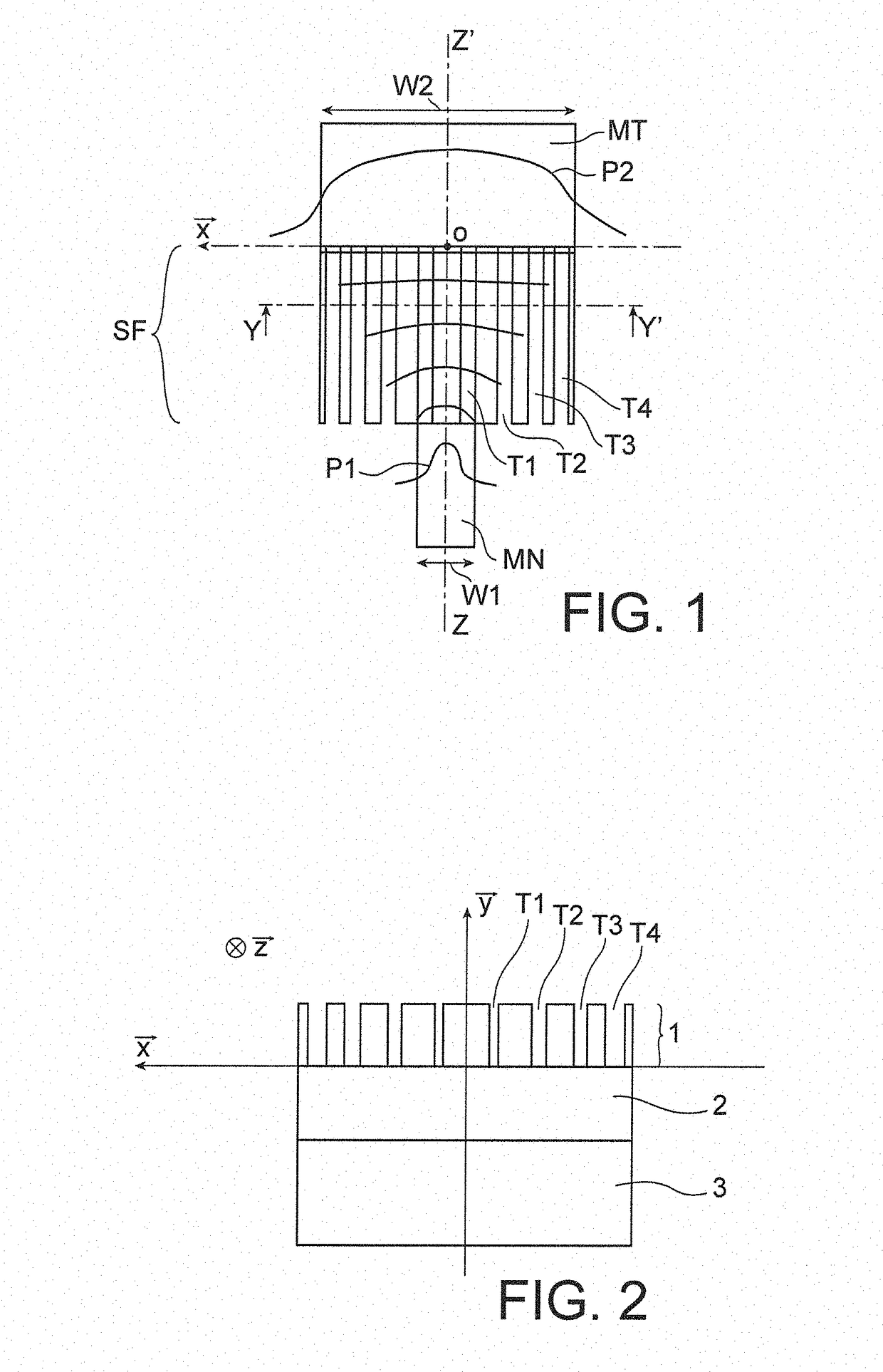
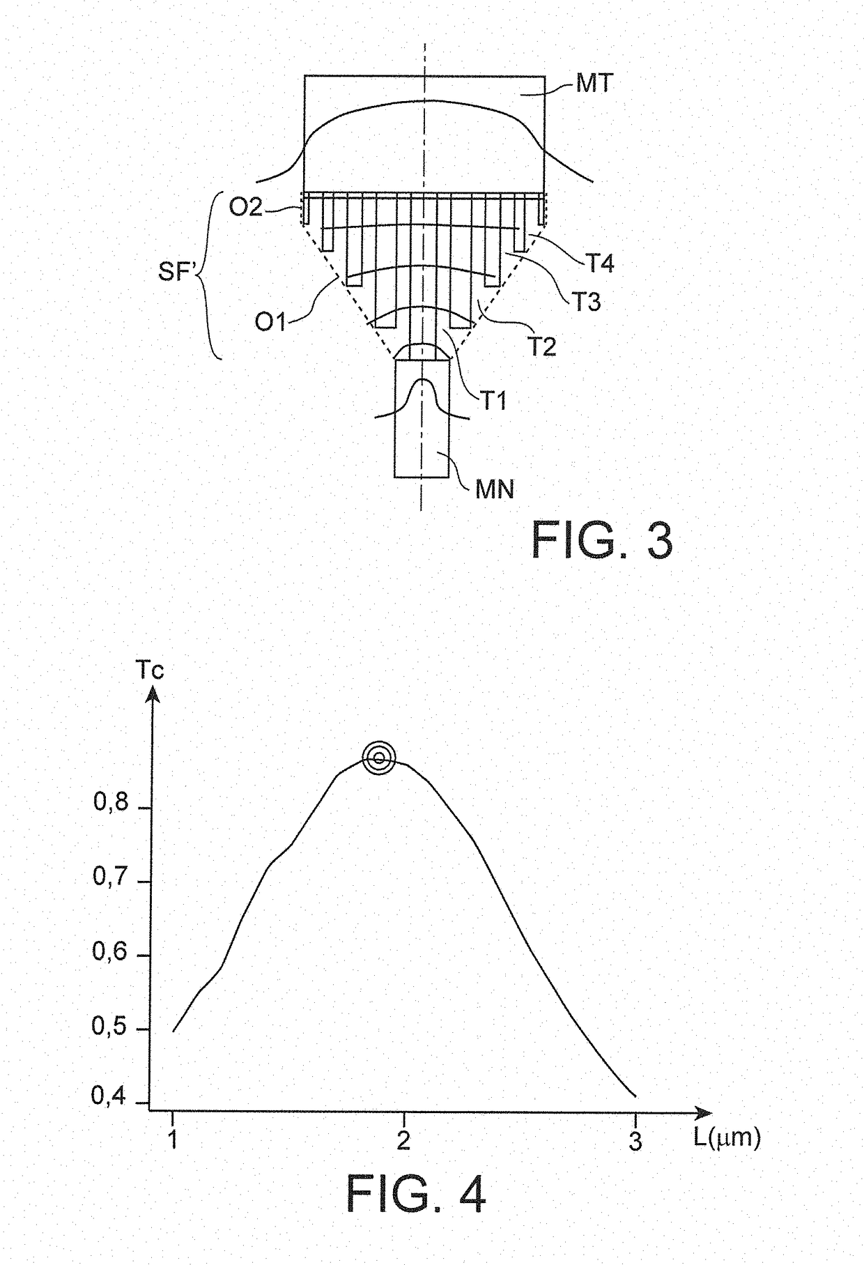
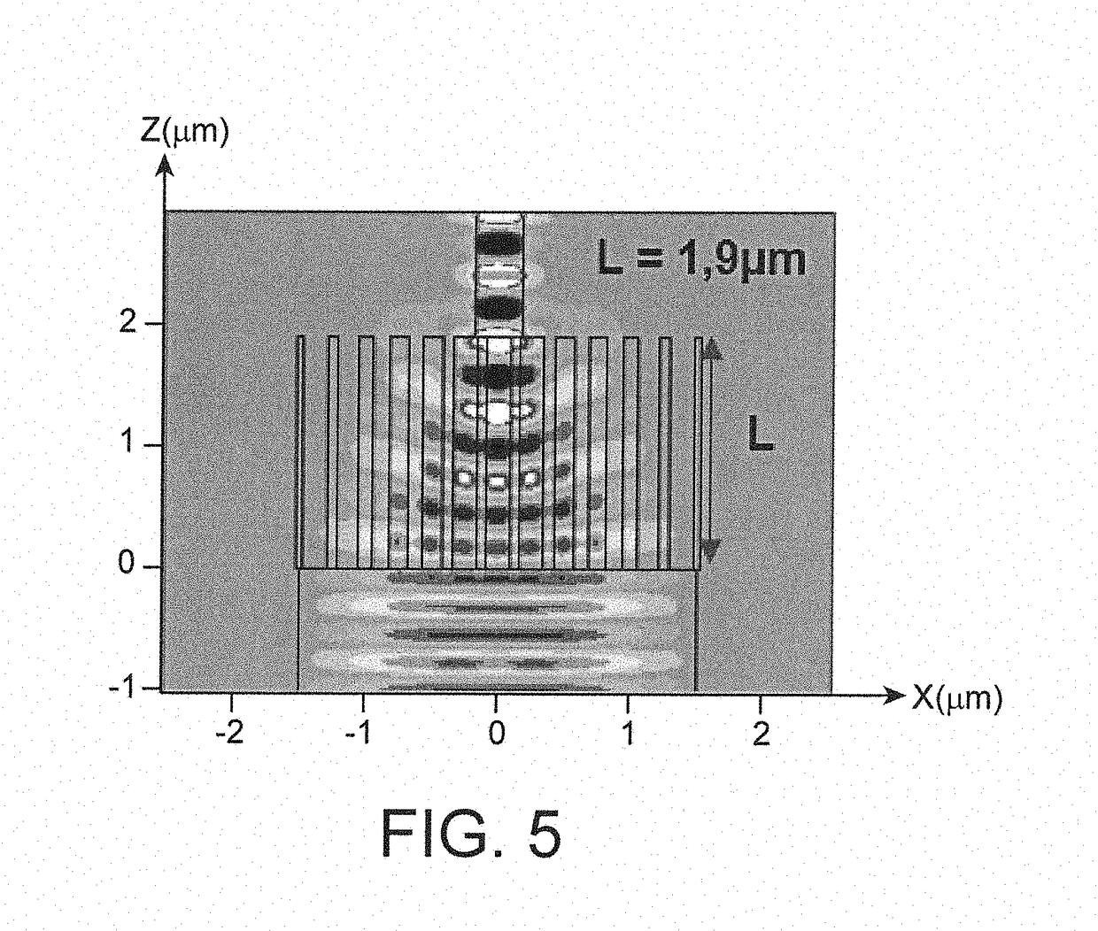
[0011]The purpose of the invention is to propose a coupling device for converting, over a short distance, light from the mode of a single-mode waveguide to the fundamental mode of a multi-mode waveguide, generally over a length that is less than the width of the multi-mode waveguide, while providing a high coupling rate.

[0012]For this purpose, the invention proposes an optical device for coupling a multi-mode waveguide to a single-mode waveguide. The device is formed in a core layer. It includes a focusing structure which comprises a plurality of trenches made in the core layer to create a pseudo graded refractive index, itself able to convert the light beam from a target mode of the multi-mode waveguide to the mode of the single-mode waveguide.

[0013]Some preferred, however non-limiting aspects of said device are described below:[0014]it is symmetrical relative to a so-called central plane, perpendicular to the core layer, the intersection whereof with the core layer comprises a dir...


PUM


Abstract

The invention relates to an optical coupling device for coupling a first waveguide, for example a multi-mode waveguide, to a second waveguide, for example a single-mode waveguide. The device is formed in a core layer and comprises a focusing structure (SF) capable of converting a light beam from a target mode of the first waveguide to a target mode of the second waveguide. The focusing structure comprises a plurality of trenches (T1-T4) made in the core layer to create a pseudo graded refractive index, itself able to convert the light beam from the target mode of the first waveguide to the target mode of the second waveguide.
The scope of the invention extends to a photonic circuit comprising a single-mode waveguide, a multi-mode waveguide and a device according to the invention for coupling the single-mode waveguide to the multi-mode waveguide. The multi-mode waveguide can comprise a surface coupling network in order to allow for coupling with an optical fibre.

Description

TECHNICAL FIELD[0001]The field of the invention is that of light guiding structures on micro- and nano-structured silicon used in photonics and optoelectronics. The invention more particularly relates to the production of a junction between a single-mode waveguide and a multi-mode waveguide, whereby such a junction is, for example, intended to allow light to be injected / extracted to / from the single-mode waveguide from / to an optical fibre by means of a surface coupling network integrated into the multi-mode waveguide.PRIOR ART[0002]The on-chip propagation of optical signals requires a good compromise between losses and compactness. Depending on the target application, the total optical path length can vary from a few millimetres for a single function (emission, modulation, filtering, photodetection) to several centimetres for the most complex circuits. In this context, silicon photonics constitutes, in addition to the compatibility thereof with electronics, an extremely efficient pla...

Claims


Application Information

Patent Timeline
IPC IPC(8): G02B6/30G02B6/14G02B6/122
CPCG02B6/305G02B2006/12095G02B6/122G02B6/14G02B6/1228G02B6/264G02B2006/12088G02B2006/1209G02B2006/12152
Inventor BOUTAMI, SALIMHASSAN, KARIM
Owner COMMISSARIAT A LENERGIE ATOMIQUE ET AUX ENERGIES ALTERNATIVES
Why Eureka
Try Eureka