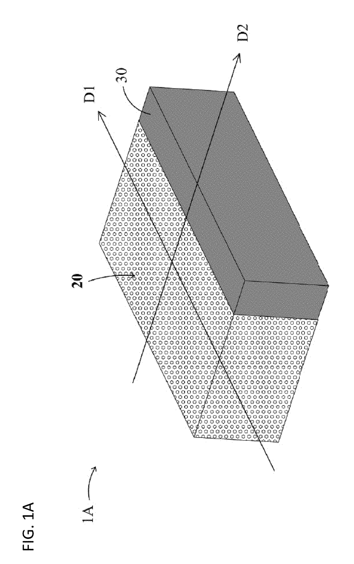
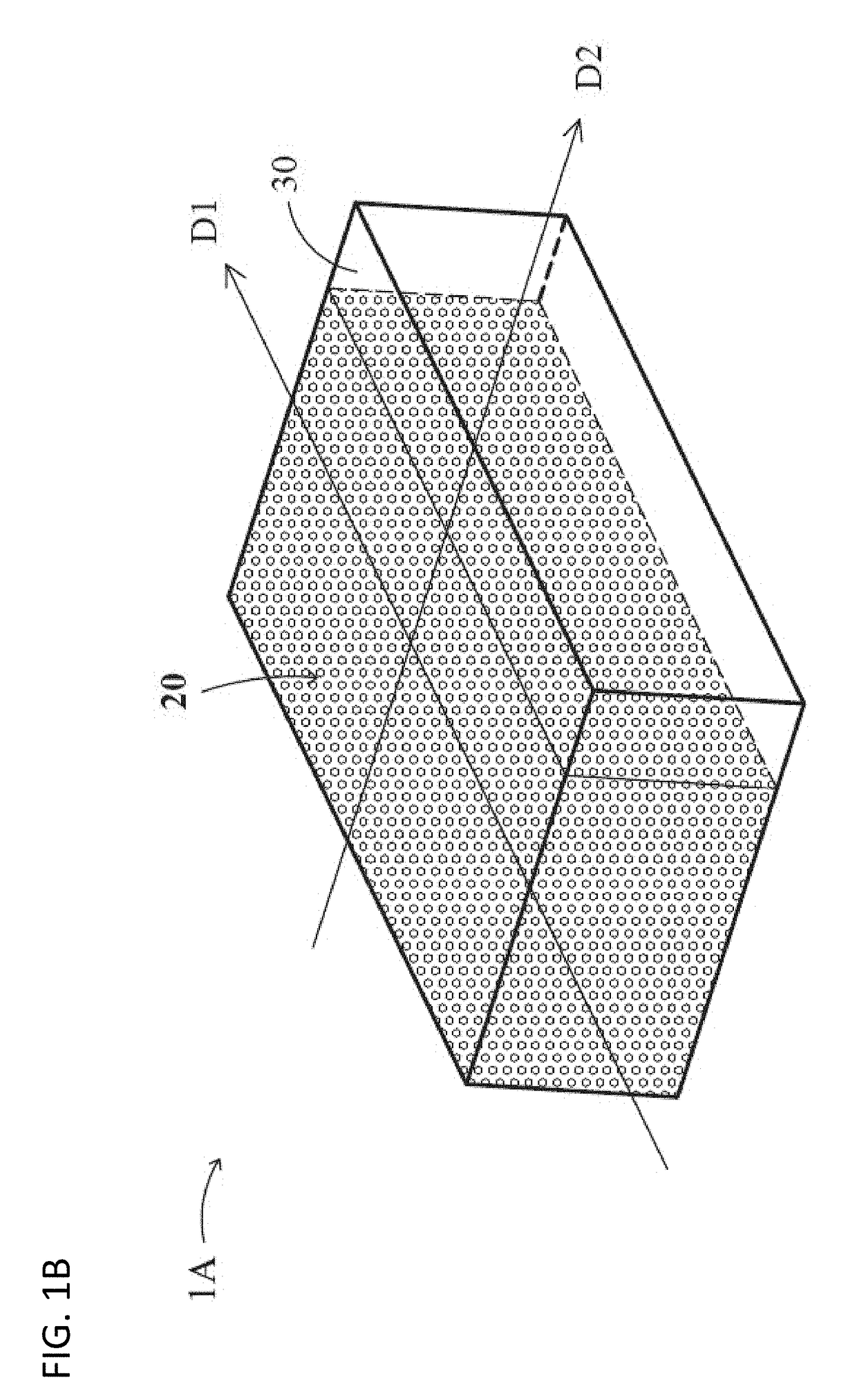
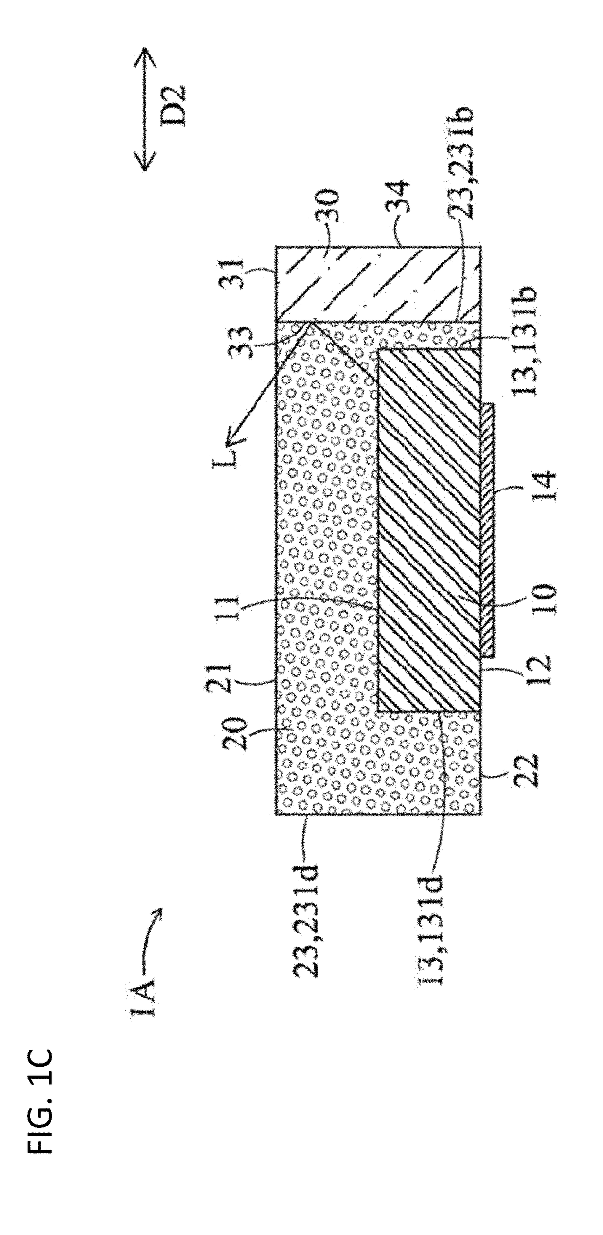
Asymmetrically shaped light-emitting device, backlight module using the same, and method for manufacturing the same

a technology of asymmetric light-emitting devices and backlight modules, applied in semiconductor devices, instruments, optics, etc., can solve the problems of increasing manufacturing costs, unable to meet some application specifications, and unable to achieve symmetric radiation patterns in led packages, etc., to achieve symmetric radiation patterns. the overall space used to achieve asymmetric radiation patterns is greatly increased, and the effect of increasing the manufacturing cos

Active Publication Date: 2019-01-24
MAVEN OPTRONICS CO LTD
View PDF0 Cites 3 Cited by
  • Summary
  • Abstract
  • Description
  • Claims
  • Application Information

AI Technical Summary

Benefits of technology

[0012]An object of some embodiments of the present disclosure is to provide a top-view CSP LED having asymmetrically shaped reflective surfaces, a backlight module including the top-view LED,...

Problems solved by technology

This type of LED packages with a symmetrical radiation pattern cannot satisfy some applications specifying an asymmetrical radiation pattern, such as street lighting.
If a PLCC-type LED package is used in applications specifying an asymmetrical radiation pattern, an extra optical lens or secondary optical lens is incorporated to shape the light to achieve a specified radiation pattern, which inevitably will increase the manufacturing cost.
Also, the overall space used to achieve an asymmetrical radiation pattern is greatly increased, which is not favorable to the design of an end product of consumer electronics nowadays.
Therefore, the LED package having an asymmetrically shaped geometry, such as a reflective cup with a partial light-transmitting structure and a partial reflective structure, is difficult to fabricate using a mass production process.
However, similar to the PLCC-type LED packages, both of the two types of CSP LEDs belong to t...

Method used


Image

  • Asymmetrically shaped light-emitting device, backlight module using the same, and method for manufacturing the same
  • Asymmetrically shaped light-emitting device, backlight module using the same, and method for manufacturing the same
  • Asymmetrically shaped light-emitting device, backlight module using the same, and method for manufacturing the same

Examples


Embodiment Construction

Definitions

[0036]The following definitions apply to some of the technical aspects described with respect to some embodiments of the disclosure. These definitions may likewise be expanded upon herein.

[0037]As used herein, the singular terms “a,”“an,” and “the” may include plural referents unless the context clearly dictates otherwise. Thus, for example, reference to a layer can include multiple layers unless the context clearly dictates otherwise.

[0038]As used herein, the term “set” refers to a collection of one or more components. Thus, for example, a set of layers can include a single layer or multiple layers. Components of a set also can be referred to as members of the set. Components of a set can be the same or different. In some instances, components of a set can share one or more common characteristics.

[0039]As used herein, the term “adjacent” refers to being near or adjoining. Adjacent components can be spaced apart from one another or can be in actual or direct contact with ...


PUM


Abstract

An asymmetrically shaped chip-scale packaging (CSP) light-emitting device (LED) includes an LED chip, a photoluminescent structure (or a light-transmitting structure), and a reflective structure. The photoluminescent structure covers the upper surface and/or the edge surface of the LED chip; and the reflective structure at least partially covers the edge surface of the photoluminescent structure. The reflective structure partially reflects the primary light emitted from the edge surface of the LED chip or the converted secondary light radiated from the edge surface of the photoluminescent structure, therefore shaping the radiation pattern asymmetrically.

Description

CROSS-REFERENCES TO RELATED APPLICATIONS[0001]This application claims the benefit of and priority to Taiwan Patent Application No. 106124542 filed on Jul. 21, 2017, and Chinese Patent Application No. 201710601827.1 filed on Jul. 21, 2017, the disclosures of which are incorporated herein by reference in their entirety.BACKGROUNDTechnical Field[0002]The present disclosure relates to a light-emitting device and a method of manufacturing the same; and more particularly relates to an asymmetrically shaped chip-scale packaging (CSP) light-emitting device (LED) used in a Liquid Crystal Display (LCD) backlight module, and a method of manufacturing the same.Description of the Related Art[0003]An LED chip is generally used as a light source for illumination, backlight, or an indicator lamp inside electronic products. Specifically, an LED chip generating a primary light is usually placed inside a package structure to form an LED package, wherein photoluminescent materials are typically dispens...

Claims


Application Information

Patent Timeline
IPC IPC(8): G02F1/1335H01L33/36H01L33/60H01L33/10
CPCG02F1/133603H01L33/36H01L33/60H01L33/10H01L33/46H01L33/508H01L33/54H01L33/58H01L2933/0025H01L2933/0058
Inventor CHEN, CHIEHCHANG, CHIA-HSIEN
Owner MAVEN OPTRONICS CO LTD
Why Eureka
Try Eureka