Supercharge Your Innovation With Domain-Expert AI Agents!

Implementing stub-less PCB vias and custom interconnect through laser-excitation conductive track structures

a technology of laser-excitation conductive track and pcb via, which is applied in the field of data processing, can solve the problems of significantly reducing the amount of total energy effectively transferred, pcb via stubs are extremely detrimental to channel margin, etc., and achieves the effects of improving yield, cost and reliability of pcbs

Inactive Publication Date: 2019-01-24
IBM CORP
View PDF3 Cites 0 Cited by
  • Summary
  • Abstract
  • Description
  • Claims
  • Application Information

AI Technical Summary

Benefits of technology

The present invention provides a method and structures for implementing stub-less printed circuit board (PCB) vias and custom interconnect through laser-excitation conductive track structures. This method and structure offer several technical advantages including greater interface margin, increased operating speed, improved yield, and reduced end-of-life failures, which can save time, money, and improve reliability of PCBs.

Problems solved by technology

PCB via stubs are extremely detrimental to channel margin.
Without removal of the unnecessary section or length of a via barrel channel margin is reduced, some amount of the propagating signal is reflected away from the intended receiver, thereby significantly reducing the amount of total energy effectively transferred.

Method used


Image

  • Implementing stub-less PCB vias and custom interconnect through laser-excitation conductive track structures
  • Implementing stub-less PCB vias and custom interconnect through laser-excitation conductive track structures
  • Implementing stub-less PCB vias and custom interconnect through laser-excitation conductive track structures

Examples


Embodiment Construction

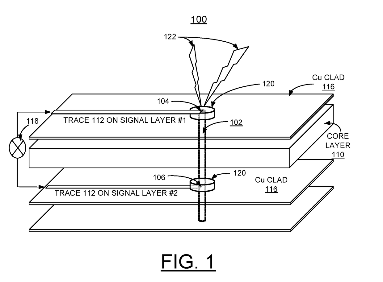
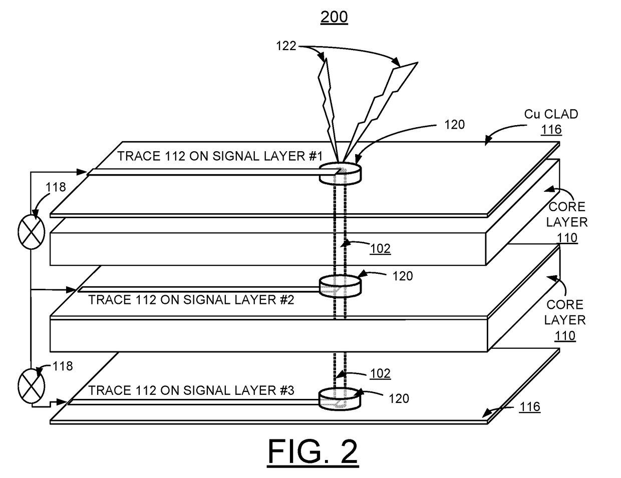
[0023]In the following detailed description of embodiments of the invention, reference is made to the accompanying drawings, which illustrate example embodiments by which the invention may be practiced. It is to be understood that other embodiments may be utilized and structural changes may be made without departing from the scope of the invention.

[0024]The terminology used herein is for the purpose of describing particular embodiments only and is not intended to be limiting of the invention. As used herein, the singular forms “a”, “an” and “the” are intended to include the plural forms as well, unless the context clearly indicates otherwise. It will be further understood that the terms “comprises” and / or “comprising,” when used in this specification, specify the presence of stated features, integers, steps, operations, elements, and / or components, but do not preclude the presence or addition of one or more other features, integers, steps, operations, elements, components, and / or gr...


PUM

PropertyMeasurementUnit
conductiveaaaaaaaaaa
resistanceaaaaaaaaaa
time domain reflectometryaaaaaaaaaa

Abstract

A method and structure are provided for implementing stub-less printed circuit board (PCB) vias and custom interconnect through laser-excitation conductive track structures. Stub-less printed PCB vias are formed which terminate at desired signal layers by controlled laser excitation without stubs or the need to back-drill to remove such stubs.

Description

FIELD OF THE INVENTION[0001]The present invention relates generally to the data processing field, and more particularly, relates to a method and structures for implementing stub-less printed circuit board (PCB) vias and custom interconnect through laser-excitation conductive track structures.DESCRIPTION OF THE RELATED ART[0002]Many computer interfaces have sufficiently high switching speed that require signal routing layer change vias without stubs. PCB via stubs are extremely detrimental to channel margin.[0003]Backdrilling is a conventional technique used to remove the via barrel stub. Without removal of the unnecessary section or length of a via barrel channel margin is reduced, some amount of the propagating signal is reflected away from the intended receiver, thereby significantly reducing the amount of total energy effectively transferred.[0004]A need exists for a method and structure for implementing stub-less printed circuit board (PCB) vias creation and custom interconnect ...

Claims


Application Information

Patent Timeline
Patent Type & Authority Applications(United States)
IPC IPC(8): H05K3/40H05K1/11H05K3/02
CPCH05K1/0251H05K3/105H05K3/4038H05K2203/107H05K2203/1136H05K3/4084H05K1/116H05K3/027B23K26/00H05K13/00
Inventor BERGE, LAYNE A.DANGLER, JOHN R.DOYLE, MATTHEW S.KUCZYNSKI, JOSEPHLIANG, THOMAS W.OROZCO, MANUEL
Owner IBM CORP
Features
  • R&D
  • Intellectual Property
  • Life Sciences
  • Materials
  • Tech Scout
  • Unparalleled Data Quality
  • Higher Quality Content
  • 60% Fewer Hallucinations
Learn More