

Thin film transistor array substrate and display panel thereof
- Summary
- Abstract
- Description
- Claims
- Application Information
AI Technical Summary
Benefits of technology
Problems solved by technology
Method used
Image

Examples
Embodiment Construction
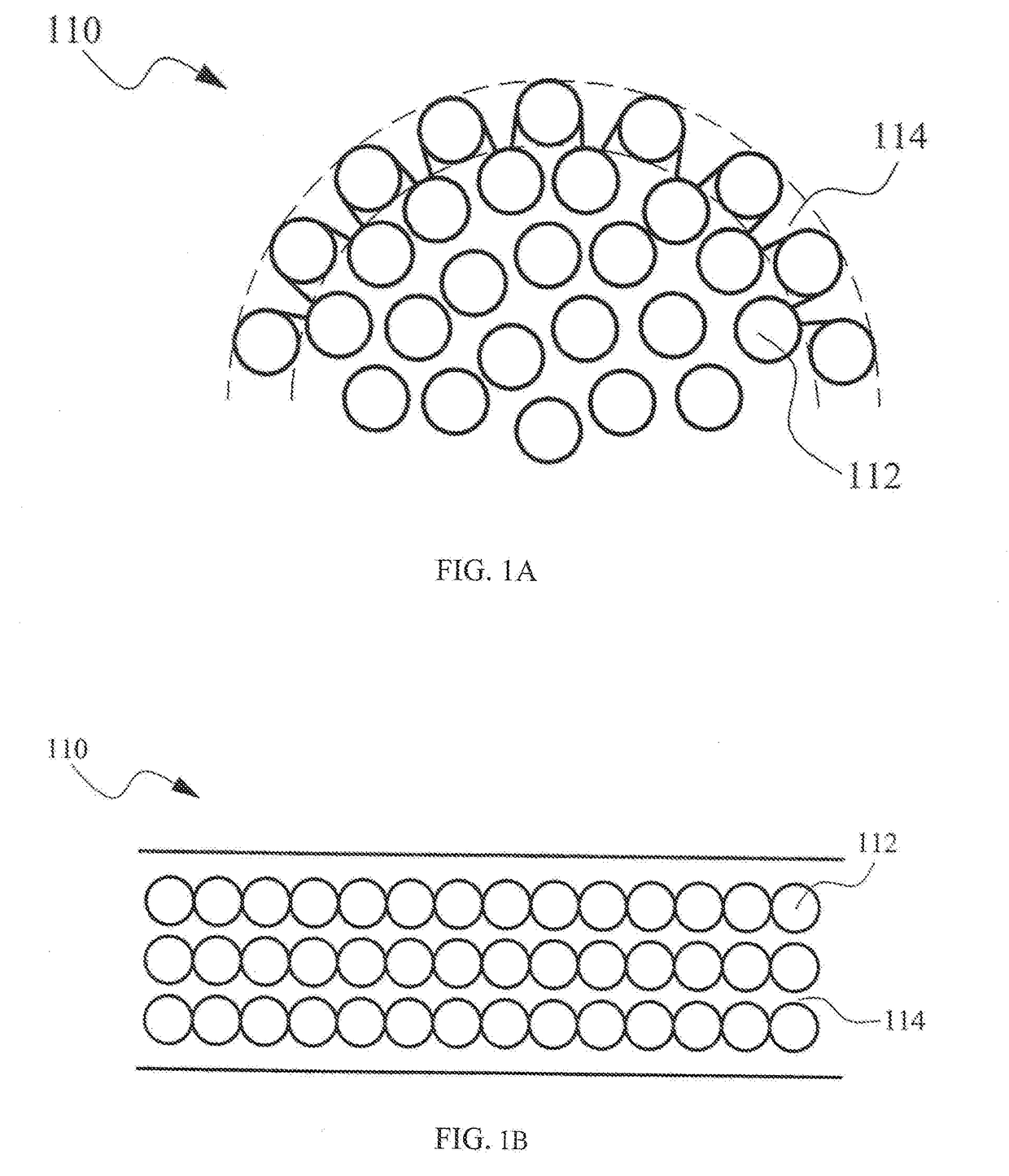
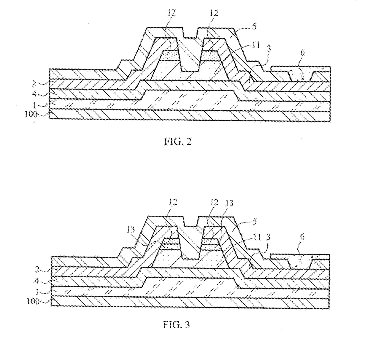
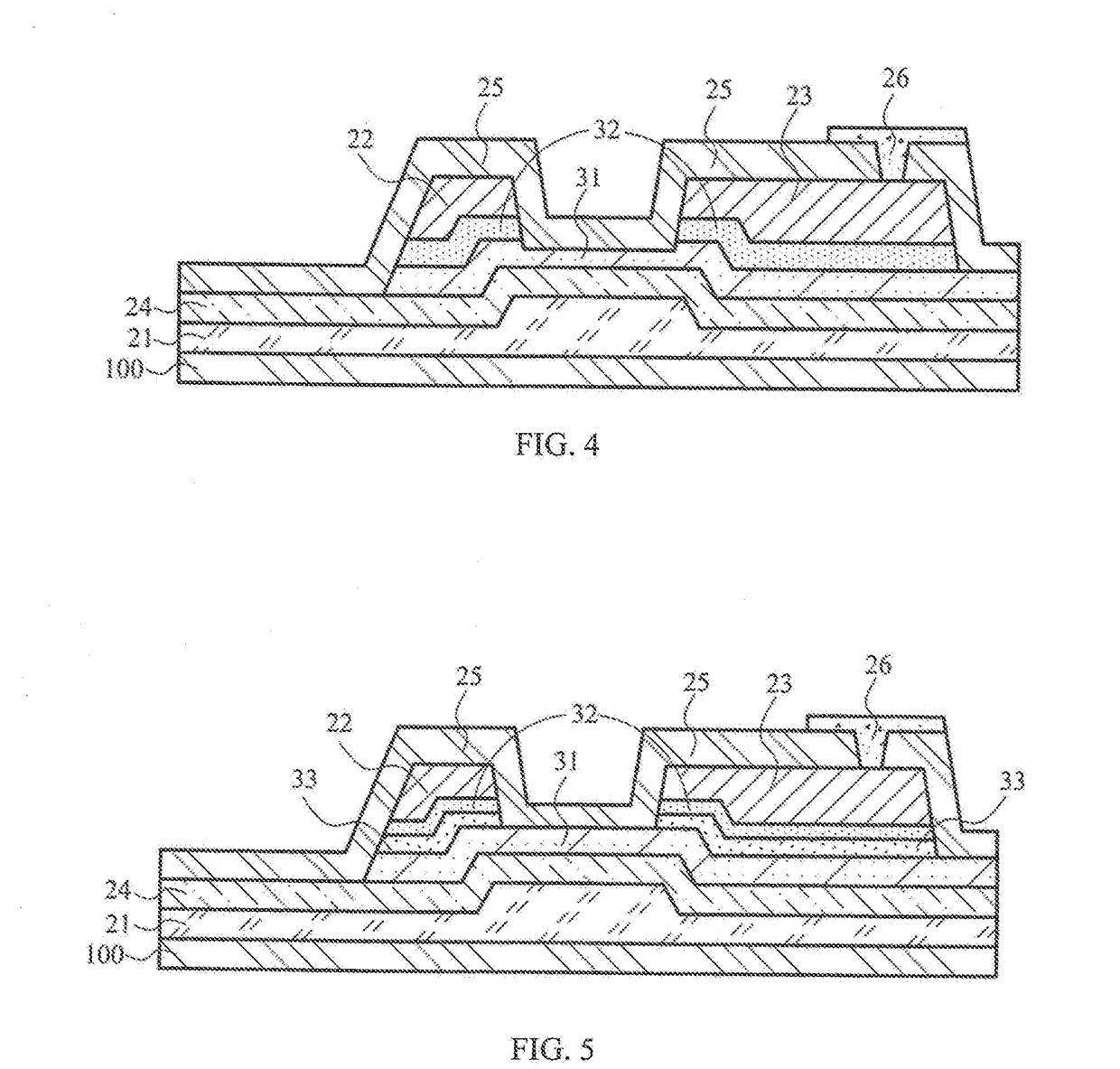
[0022]The following embodiments are referring to the accompanying drawings for exemplifying specific implementable embodiments of the present invention. Furthermore, directional terms described by the present invention, such as upper, lower, front, back, left, right, inner, outer, side and etc., are only directions by referring to the accompanying drawings, and thus the used directional terms are used to describe and understand the present invention, but the present invention is not limited thereto.
[0023]The drawings and description are to be regarded as illustrative in nature and not restrictive. Like reference numerals designate like elements throughout the specification. In addition, the size and thickness of each component shown in the drawings are arbitrarily shown for understanding and ease of description, but the present invention is not limited thereto.
[0024]In the drawings, the thickness of layers, films, panels, regions, etc., are exaggerated for clarity. In the drawings, ...
PUM
 Abstract
Description
Claims
Application Information