

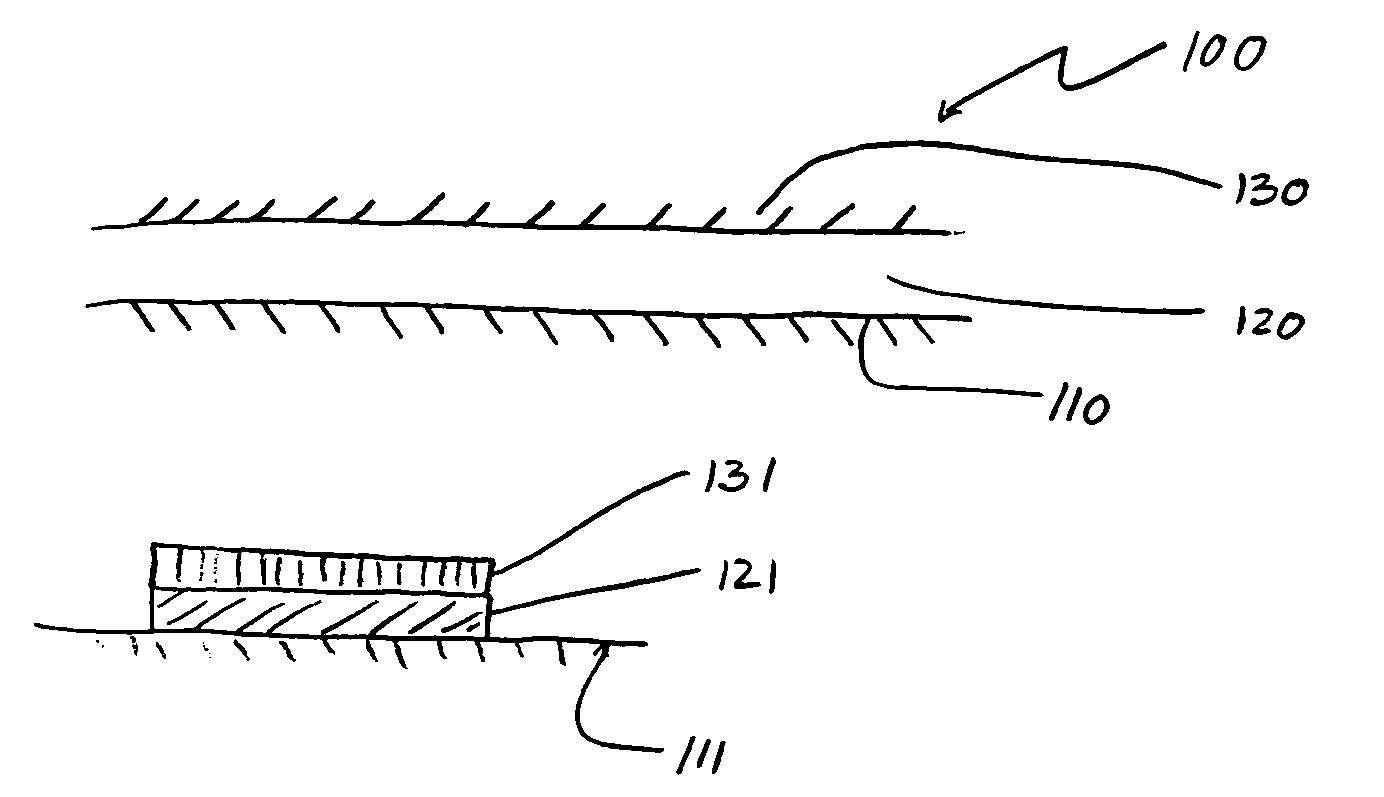
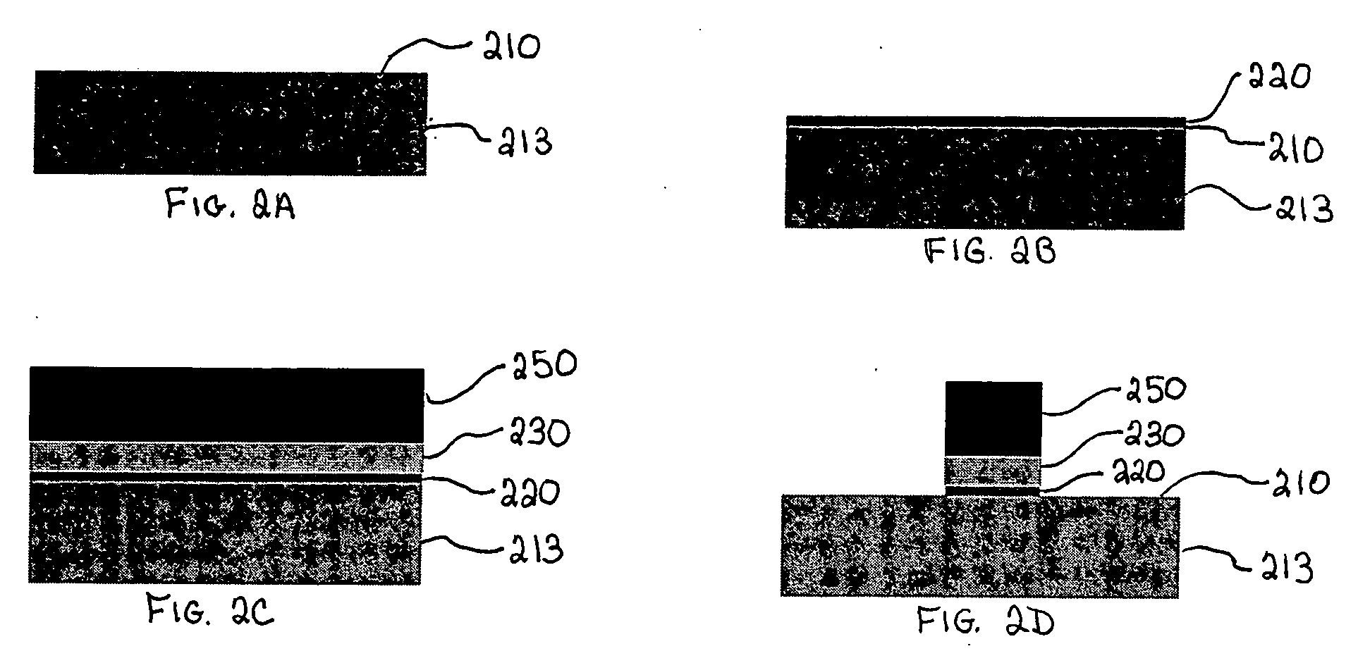
Method for forming an interface between germanium and other materials
- Summary
- Abstract
- Description
- Claims
- Application Information
AI Technical Summary
Benefits of technology
Problems solved by technology
Method used
Image

Examples
example 1
Germanium Schottky Diodes
[0053] Schottky diodes were produced using crystal germanium substrates. Surfaces of the substrates were cleaned by cyclically exposing the surfaces to either hydrogen fluoride or hydrogen chloride, followed by a deionized water (DI water) rinse, to remove the presence of germanium oxide. The surfaces were subsequently exposed to a ammonium sulfide ((NH4)2S) solution at a temperature between 60° C. and 70° C. for 20 minutes to form interfacial layers on the surfaces. The layers were again rinsed with DI water. Evaporated titanium is then deposited on the interfacial layers to form the Schottky diodes.
example 2
Interfacial Layer Hinderance of Germanium Oxide Formation
[0054] The effect of the interfacial layer in hindering oxide formation was examined using X-ray photoelectron spectroscopy (XPS). Two surfaces were tested using XPS. A control surface of germanium was prepared by immersing the surface in a solution having a 4:1 ratio of DI water to hydrogen chloride. A sulfur treated surface of germanium was prepared by utilizing the hydrogen chloride procedure for the control surface, followed by immersing the surface in a 20% solution of ammonium sulfide at 65° C. for 20 minutes. The surface was subsequently cleaned with DI water. XPS was then conducted on each surface to detect the presence of germanium oxide. XPS impinges photons on a surface to excite and cause photoelectrons to be ejected from the surface. The photoelectrons are collected and their individual energies are determined, the spectra determining the nature of the material surface. For the measurements conducted here the pho...
example 3
Comparing IV Characteristics of Schottky Diodes
[0056] Two Schottky diodes were manufactured and their current vs. voltage (IV) characteristics compared. Two germanium substrates were cleaned using dilute hydrofluoric acid. One of the substrates was subsequently immersed in ammonium sulfide at 65° C. for 20 min. The other substrate, acting as a control, was not exposed to sulfur. Both substrates were then loaded into an e-beam evaporator and platinum electrodes were shadow masked onto the germanium substrates. Aluminum was evaporated onto the back of the samples for backside electrical contact. The platinum electrode area was 1.95 E-3 cm2.
[0057]FIG. 7 shows current vs. voltage characteristics for each of the devices. Trace 710 shows the current vs. voltage characteristics of the sulfur-treated device, while trace 720 shows the characteristics of the control device. Under conditions of forward biasing, the sulfur treated device has improved current transmission at a given voltage re...
PUM
 Abstract
Description
Claims
Application Information