Organic Transistor, Compound, Organic Semiconductor Material for Non-Light-Emitting Organic Semiconductor Device, Material for Organic Transistor, Coating Solution for Non-Light-Emitting Organic Semiconductor Device, and Organic Semiconductor Film for Non-Light-Emitting Organic Semiconductor Device

Inactive Publication Date: 2016-10-13
FUJIFILM CORP
View PDF2 Cites 1 Cited by
  • Summary
  • Abstract
  • Description
  • Claims
  • Application Information

AI Technical Summary

Benefits of technology

[0101]According to the present invention, it is possible to provide a compound, which can improve carrier mobility when being used in a semiconducto

Problems solved by technology

Being useful as an organic EL element material does not mean being useful as a semiconductor material for an organic transistor, because the characteristics required for the organic compound vary between the organic EL element and the organic transistor.
Generally, an organic compound having high crystallinity causes luminescence defectiveness such as nonuniform in-plane electric field intensity, nonuniform luminescence, and quenching of luminescence.
Consequently, the use of the organic compound constituting the organic EL element material as an organic semiconductor material does not ensure that excellent transistor characteristics can be obtained.
In addition, likewise, being useful as a solar cell material does not mean being useful as a semiconductor material for an organic transistor for which extremely

Method used


Image

  • Organic Transistor, Compound, Organic Semiconductor Material for Non-Light-Emitting Organic Semiconductor Device, Material for Organic Transistor, Coating Solution for Non-Light-Emitting Organic Semiconductor Device, and Organic Semiconductor Film for Non-Light-Emitting Organic Semiconductor Device
  • Organic Transistor, Compound, Organic Semiconductor Material for Non-Light-Emitting Organic Semiconductor Device, Material for Organic Transistor, Coating Solution for Non-Light-Emitting Organic Semiconductor Device, and Organic Semiconductor Film for Non-Light-Emitting Organic Semiconductor Device
  • Organic Transistor, Compound, Organic Semiconductor Material for Non-Light-Emitting Organic Semiconductor Device, Material for Organic Transistor, Coating Solution for Non-Light-Emitting Organic Semiconductor Device, and Organic Semiconductor Film for Non-Light-Emitting Organic Semiconductor Device

Examples


example 1

Synthesis Example 1

Synthesis of Compounds 1 to 3, 5, 11, 13, 15, 16, 24, 31, and 32 and Intermediate Compounds e, f, and g

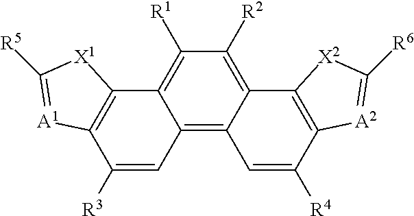
[0340]According to a specific synthesis procedure shown in the following scheme 1, compounds 1 to 3, 5, 11, 13, 15, 16, 24, 31, and 32 as the compound represented by Formula (1) and intermediate compounds e, f, and g were synthesized.

[0341]A process will be specifically described in which the intermediate compound e represented by Formula (3), the intermediate compound f represented by Formula (3), and then the intermediate compound g represented by (3) are synthesized from the following compound d.

[0342](Synthesis of Compound e)

[0343]5.0 g (12.82 mmol) of the compound d was dissolved in 40 ml of N,N′-dimethylacetamide, 360.0 mg (0.51 mmol) of PdCl2(PPh3)2 was added thereto in a nitrogen atmosphere, and then the resulting solution was heated to an internal temperature of 80° C. After 4 hours, the solution was left to cool to room temperature, and 1 N HCl and ethy...

example 2

Preparation / Evaluation of Element

[0358]All of the materials used for preparing elements were purified by sublimation. Through high-performance liquid chromatography (TOSOH CORPORATION, TSKgel ODS-100Z), it was confirmed that the materials had purity (area ratio for absorption intensity at 254 nm) of equal to or higher than 99.5%.

[0359]

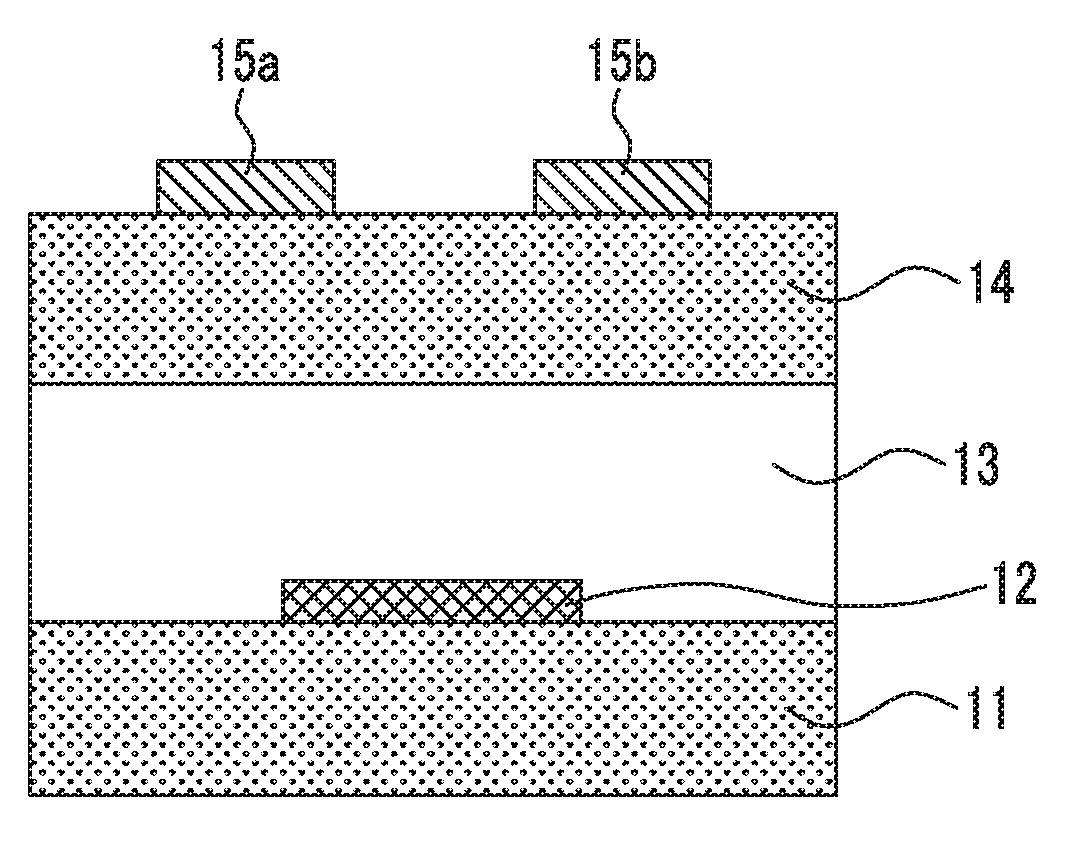
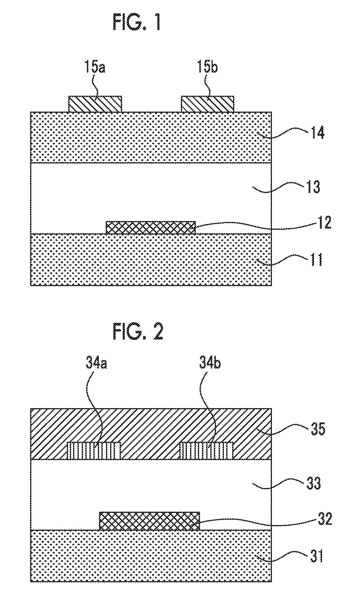
[0360]Each of the compounds of the present invention or the comparative compounds (1 mg each) was mixed with toluene (1 mL) and heated to 100° C., thereby obtaining a coating solution for a non-light-emitting organic semiconductor device. In a nitrogen atmosphere, the coating solution was cast onto a substrate for measuring FET characteristics that was heated to 90° C., thereby forming an organic semiconductor film for a non-light-emitting organic semiconductor device. In this way, an organic transistor element of Example 2 for measuring FET characteristics was obtained. As the substrate for measuring FET characteristics, a silicon substrate comprising...

example 3

Formation of Semiconductor Active Layer (Organic Semiconductor Layer) by Using Compound and Binder Together

[0380]Each of the compounds of the present invention or the comparative compounds (1 mg each) was mixed with 1 mg of PαMS (poly(α-methylstyrene, Mw=300,000), manufactured by Sigma-Aldrich Co, LLC.) and toluene (1 mL), and the mixture was heated to 100° C., thereby obtaining a coating solution. Organic transistor elements for measuring FET characteristics were prepared and evaluated in the same manner as in Example 2, except that the coating solution obtained as above was used.

[0381]The obtained results are shown in the following Table 2.

TABLE 2ThresholdOrganicCarriervoltage shiftsemiconductormobilityafter repeatedElement No.material(cm2 / Vs)drivingNoteElement 12Compound 18.5 × 10⁻²APresentinventionElement 13Compound 51.5 × 10⁻¹APresentinventionElement 14Compound 117.1 × 10⁻²APresentinventionElement 15Compound 168.4 × 10⁻²APresentinventionComparativeComparative3.0 × 10−5CComparat...


PUM


Abstract

Provided are an organic transistor containing a compound represented by the following formula in a semiconductor active layer; a compound which improves carrier mobility when being used in a semiconductor layer of an organic transistor and exhibits high solubility in an organic solvent; an organic semiconductor material for a non-light-emitting organic semiconductor device; a material for an organic transistor; a coating solution for a non-light-emitting organic semiconductor device; and an organic semiconductor film for a non-light-emitting organic semiconductor device (each of X1 and X2 represents NR13, an O atom, or a S atom; A1 represents CR7 or a N atom; A2 represents CR8 or a N atom; R13 represents a hydrogen atom, an alkyl group, an alkenyl group, an alkynyl group, or an acyl group; each of R1 to R8 independently represents a hydrogen atom or a substituent; at least one of R1, R2, R3, R4, R5, R6, R7, or R8 is a substituent represented by -L-R; L represents a divalent linking group having a specific structure; and R represents an alkyl group, a cyano group, a vinyl group, an ethynyl group, an oxyethylene group, an oligo-oxyethylene group in which a repetition number v of an oxyethylene unit is equal to or greater than 2, a siloxane group, an oligosiloxane group having two or more silicon atoms, or a trialkylsilyl group).

Description

CROSS-REFERENCE TO RELATED APPLICATIONS[0001]This application is a Continuation of PCT International Application No. PCT / JP2014 / 083194, filed on Dec. 16, 2014, which claims priority under 35 U.S.C. Section 119(a) to Japanese Patent Application No. 2013-265910 filed on Dec. 24, 2013. Each of the above applications is hereby expressly incorporated by reference, in its entirety, into the present application.BACKGROUND OF THE INVENTION[0002]1. Field of the Invention[0003]The present invention relates to an organic transistor, an organic semiconductor film, an organic semiconductor material, and the like. Specifically, the present invention relates to a compound having a phenanthrene skeletal structure condensed with two 5-membered heterocyclic rings, an organic transistor containing the compound, an organic semiconductor material for a non-light-emitting organic semiconductor device that contains the compound, a material for an organic transistor that contains the compound, a coating so...

Claims


Application Information

Patent Timeline
IPC IPC(8): H01L51/00C07D487/04
CPCH01L51/0072H01L51/055H01L51/0558C07D487/04C07D333/18C07D493/04C07D495/04C09B57/00C09B67/009H10K85/653H10K85/656H10K85/654H10K85/655H10K85/6576H10K10/488H10K10/484H10K85/6572H10K10/481
Inventor YOUFU, KATSUYUKIHIRAI, YUKIMASUI, KENSUKE
Owner FUJIFILM CORP
Why Eureka
Try Eureka