Touch display panel and touch display device

a touch display panel and touch display technology, applied in the field of touch display panel and touch display device, can solve problems such as noise on touch sensing signals, and achieve the effects of preventing direct capacitance, preventing capacitance formation, and large capacitan

Active Publication Date: 2019-03-14
LG DISPLAY CO LTD
View PDF3 Cites 13 Cited by
  • Summary
  • Abstract
  • Description
  • Claims
  • Application Information

AI Technical Summary

Benefits of technology

[0015]According to the embodiments of the present disclosure, by arranging a shielding structure in a region where a touch line and a data line overlap each other, it is possible to prevent direct capacitance from being formed between the touch line and the data line.
[0016]In addition, by connecting the shielding structure to a touch electrode that forms relatively large capacitance, it is possible to prevent capacitance formed between the shielding structure and the data line from affecting a touch sensing signal transmitted through the touch line.
[0017]Accordingly, it is possible to prevent capacitance formed between the data line and the touch line from causing interference that will be seen as noise on a touch sensing signal and thus improve touch sensing performance.
[0018]Further, by providing a structure in which the shielding structure is formed on the same layer as the touch electrode or the pixel electrode, it is easy to configure a structure for reducing noise on a touch sensing signal.
[0019]Further, by disposing the touch load reduction layer between the shielding structure and the touch line, it is possible to reduce noise caused by capacitance between the touch line and the non-overlapped data line.
[0020]As described above, by removing the influence of display noise on a touch sensing signal, touch sensing can be performed independently of display driving.

Problems solved by technology

There is a problem in that such capacitance may cause noise on a touch sensing signal.

Method used


Image

  • Touch display panel and touch display device
  • Touch display panel and touch display device
  • Touch display panel and touch display device

Examples


first embodiment

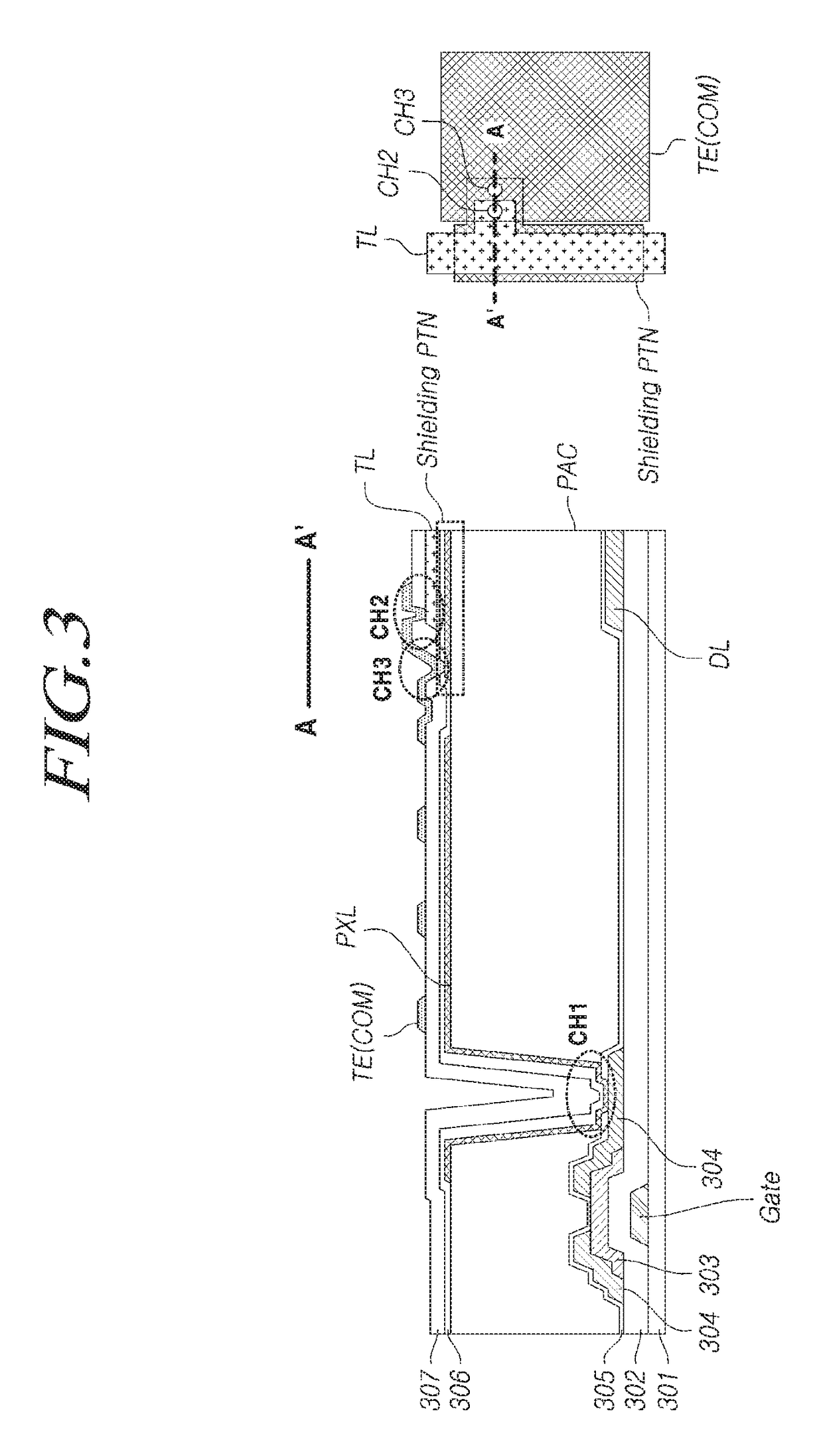
[0070]Referring to FIG. 3, in the touch display device 100 a gate electrode Gate is disposed on a substrate 301, and a gate insulating layer 302 is disposed on the gate electrode Gate.

[0071]An active layer 303, a source / drain electrode 304, and a data line DL are disposed on the gate insulating layer 302.

[0072]A first protective layer 305 is disposed on the source / drain electrode 304 and the data line DL, and a planarization layer PAC is disposed on the first protective layer 305. The first protective layer 305 and the planarization layer PAC may be formed of an insulating material.

[0073]A pixel electrode PXL may be disposed on the planarization layer PAC, and the pixel electrode PXL may be connected to the source / drain electrode 304 via a first contact hole CH1.

[0074]In addition, a second protective layer 306, a touch line TL, a third protective layer 307, and a touch electrode TE may be sequentially disposed on the pixel electrode PXL. Here, the touch electrode TE may be a common...

second embodiment

[0094]FIG. 5 illustrates a portion where a touch line TL and a touch electrode TE are connected in the touch display device 100 and FIG. 6 illustrates a portion where a touch line TL and a touch electrode TE are not connected to each other.

[0095]Referring to FIG. 5, in the touch display device 100 according to the second embodiment, a gate electrode Gate is disposed on a substrate 301, and a gate insulating layer 302 is disposed on the gate electrode Gate.

[0096]An active layer 303, a source / drain electrode 304, a data line DL, and a first protective layer 305 are disposed on the gate insulating layer 302.

[0097]A planarization layer PAC is disposed on the first protective layer 305, and a touch electrode TE, i.e., a common electrode TE (COM), is disposed on the planarization layer PAC.

[0098]A second protective layer 306, a touch line TL, a third protective layer 307, and a pixel electrode PXL are sequentially disposed on the touch electrode TE, and the pixel electrode PXL is connect...

third embodiment

[0107]FIG. 7 illustrates a portion where a touch line TL and a touch electrode TE are connected in the touch display device 100 and FIG. 8 illustrates a portion where a touch line TL and a touch electrode TE are not connected to each other.

[0108]Referring to FIG. 7, in the touch display device 100 according to the third embodiment, a gate electrode Gate is disposed on a substrate 301, and a gate insulating layer 302 is disposed on the gate electrode Gate.

[0109]An active layer 303, a source / drain electrode 304, a data line DL, and a first protective layer 305 are disposed on the gate insulating layer 302.

[0110]A planarization layer PAC is disposed on the first protective layer 305 and a pixel electrode PXL is disposed on the planarization layer PAC.

[0111]The pixel electrode PXL may be connected to the source / drain electrode 304 via a first contact hole CH1.

[0112]A second protective layer 306 is disposed on the pixel electrode PXL, and a touch electrode TE is disposed on the second p...


PUM


Abstract

Embodiments disclosed herein relate to a touch display panel and a touch display device. By arranging a shielding structure, which is connected to a touch electrode in a region where a touch line and a data line overlap each other or is applied with a shielding signal corresponding to a touch driving signal from an outside circuit, between the touch line and the data line, it is possible to prevent direct capacitance from being formed between the touch line and the data line, and to prevent the capacitance formed due to the data line from causing noise on a touch sensing signal. In addition, by arranging a touch load reduction layer between the shielding structure and the touch line, it is also possible to reduce the capacitance between the touch line and the data line arranged in the horizontal direction, thereby improving touch sensing performance.

Description

CROSS REFERENCE TO RELATED APPLICATIONS[0001]This application claims priority from Korean Patent Application No. 10-2017-0115303, filed Sep. 8, 2017, and Korean Patent Application No. 10-2018-0081639, filed Jul. 13, 2018, which is hereby incorporated by reference for all purposes as if fully set forth herein.BACKGROUNDTechnical Field[0002]Embodiments disclosed herein relate to a touch display panel and a touch display device.Description of the Related Art[0003]As society has developed into an information-based society, demand for a display device for displaying images is increasing, and various types of display devices such as a liquid crystal display, a plasma display, and an organic light-emitting display are being utilized.[0004]In order to provide more various functions, such display devices provide functions of recognizing a user's touch on a display panel and performing an input process based on the recognized touch.[0005]A display device capable of performing touch recognitio...

Claims


Application Information

Patent Timeline
Patent Type & Authority Applications(United States)
IPC IPC(8): G06F3/041G06F3/044G06F3/047G09G3/20
CPCG06F3/0412G06F3/044G06F3/047G09G3/2096G06F3/0416G02F1/13338G09G2354/00G02F2201/123G06F2203/04107G06F2203/04111G06F3/0443G06F3/04164G02F1/13606
Inventor KIM, HOONBAEKIM, CHEOLSESHIN, SEUNGMOKKIM, JUHANPARK, YONGCHANPARK, HYUNHO
Owner LG DISPLAY CO LTD
Why Eureka
Try Eureka