Unlock instant, AI-driven research and patent intelligence for your innovation.

Stacked memory device, a system including the same and an associated method

Active Publication Date: 2019-03-28
SAMSUNG ELECTRONICS CO LTD
View PDF0 Cites 20 Cited by
  • Summary
  • Abstract
  • Description
  • Claims
  • Application Information

AI Technical Summary

Benefits of technology

The patent describes a stacked memory device that includes a logic die and multiple memory dies which perform calculations based on broadcast data and internal data. The broadcast data is commonly provided to the calculation dies through through-silicon vias, while the internal data is read from the memory circuits of the calculation dies. The device can perform additional calculations simultaneously using the multiple calculation units. The invention also includes a memory system with a base substrate and at least one logic semiconductor die stacked together with multiple memory semiconductor dies, and a plurality of calculation units formed in the memory semiconductor dies. The technique provides efficient data processing and faster calculations.

Problems solved by technology

Memory bandwidth and latency are performance bottlenecks in many processing systems.
Such stacking technology may increase memory capacity and also suppress bandwidth and latency penalties.
In this case, however, inter-device bandwidth and inter-device latency penalties may happen twice in each access.
Accordingly, the inter-device bandwidth and inter-device latency can have a significant impact on processing efficiency and power consumption when the external device requests multiple accesses to the stacked memory device.

Method used


Image

  • Stacked memory device, a system including the same and an associated method
  • Stacked memory device, a system including the same and an associated method
  • Stacked memory device, a system including the same and an associated method

Examples


Embodiment Construction

[0026]Exemplary embodiments of the present inventive concept will be described more fully hereinafter with reference to the accompanying drawings. In the drawings, like numerals may refer to like elements.

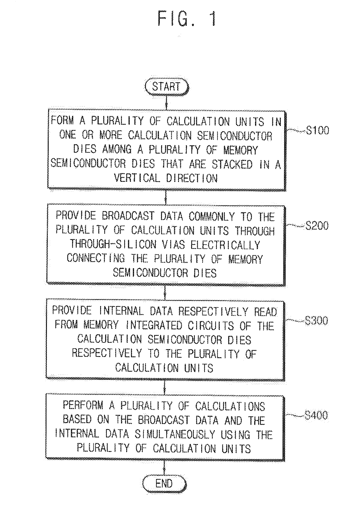
[0027]FIG. 1 is a flow chart illustrating a method of operating a stacked memory device according to an exemplary embodiment of the inventive concept.

[0028]Referring to FIG. 1, a plurality of calculation units are formed in one or more calculation semiconductor dies among a plurality of memory semiconductor dies that are stacked in a vertical direction (S100). Broadcast data are provided commonly to the plurality of calculation units by using through-silicon vias electrically connecting the plurality of memory semiconductor dies to each other (S200). Internal data respectively read from memory integrated circuits of the calculation semiconductor dies are provided respectively to the plurality of calculation units (S300). A plurality of calculations are simultaneously performed base...


PUM


Abstract

A stacked memory device includes; a logic semiconductor die; a plurality of memory semiconductor dies stacked with the logic semiconductor die, wherein each of the memory semiconductor dies includes a memory integrated circuit and one or more of the memory semiconductor dies is a calculation semiconductor die including a calculation unit; and through-silicon vias electrically connecting the logic semiconductor die and the plurality of memory semiconductor dies, wherein each of the calculation units is configured to perform calculations based on broadcast data and internal data and to generate calculation result data, wherein the broadcast data is commonly provided to the calculation semiconductor dies through the through-silicon vias, and the internal data is respectively read from the memory integrated circuits of the calculation semiconductor dies.

Description

CROSS-REFERENCE TO RELATED APPLICATION[0001]This U.S. Non-provisional application claims priority under 35 U.S.C. § 119 to Korean Patent Application No. 10-2017-0125481, filed on Sep. 27, 2017, in the Korean Intellectual Property Office (KIPO), the disclosure of which is incorporated by reference herein in its entirety.TECHNICAL FIELD[0002]The present inventive concept relates to semiconductor integrated circuits, and more particularly, to a stacked memory device, a system including a stacked memory device and a method of operating a stacked memory device.DISCUSSION OF THE RELATED ART[0003]Memory bandwidth and latency are performance bottlenecks in many processing systems. Memory capacity may be increased by using a stacked memory device in which a plurality of semiconductor devices are stacked in a memory chip package. The stacked semiconductor devices (or dies) may be electrically connected to each other by through-silicon vias or through-substrate vias (TSVs). Such stacking techn...

Claims


Application Information

Patent Timeline
IPC IPC(8): G11C7/10G06F12/06G11C7/22G11C7/06G06F3/06G06F7/523
CPCG11C7/1078G06F12/0646G11C7/22G11C7/06G06F3/0611G06F3/0625G06F7/523G06F3/0659H01L23/481H01L24/24H01L25/18H01L2224/24145H01L2924/181H01L2224/16225H01L2924/15311G11C5/04G11C5/063G11C5/066G11C7/1006G11C7/1048G11C7/1069G11C7/1096G11C2207/2272Y02D10/00H01L2924/00012G11C5/06G11C7/10G11C8/12
Inventor SHIN, HYUN-SUNGCHOI, IK-JOONKIM, SO-YOUNGBYUN, TAE-KYUYOUN, JAE-YOUN
Owner SAMSUNG ELECTRONICS CO LTD