Semiconductor device module
a technology of semiconductor devices and devices, applied in semiconductor devices, semiconductor/solid-state device details, electrical apparatus, etc., can solve the problems of reducing increasing the stress of the power device, etc., to improve the positional precision of the lead electrode, and improve the reliability of the semiconductor device module
- Summary
- Abstract
- Description
- Claims
- Application Information
AI Technical Summary
Benefits of technology
Problems solved by technology
Method used
Image

Examples
embodiment 1
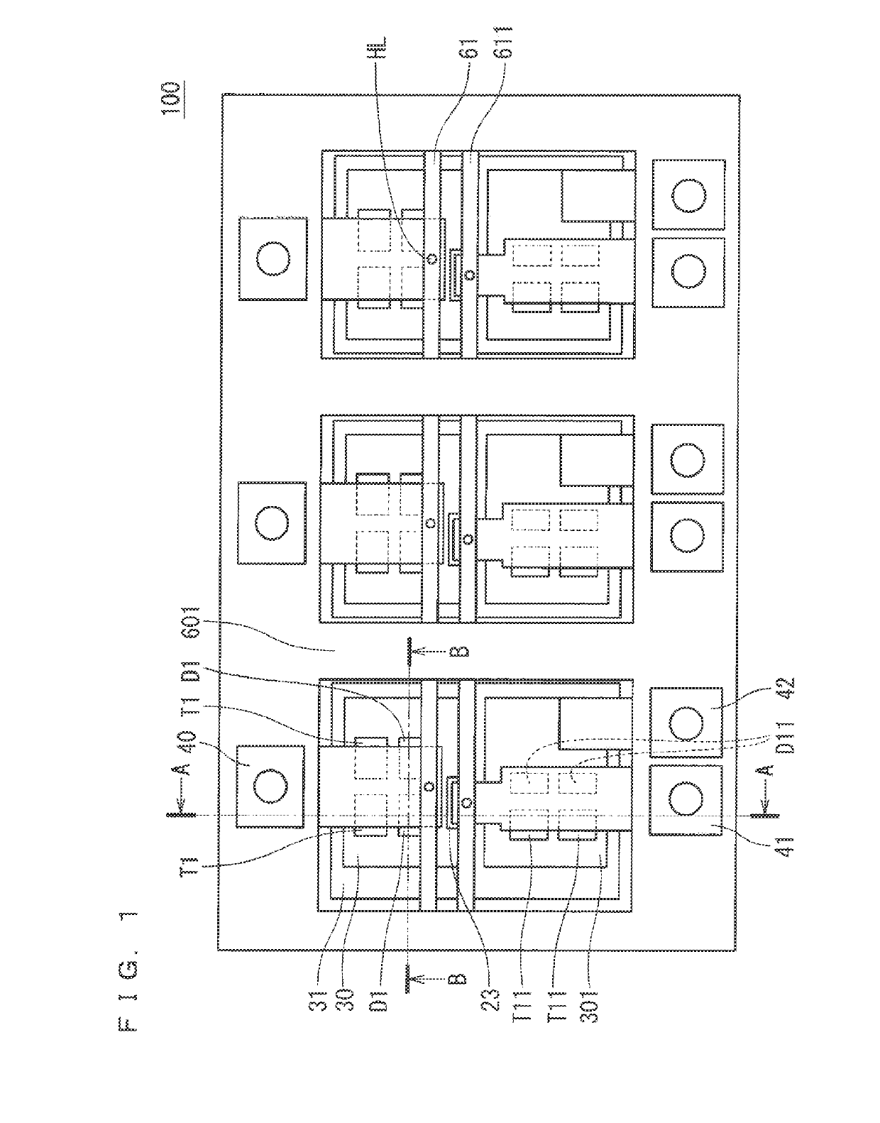
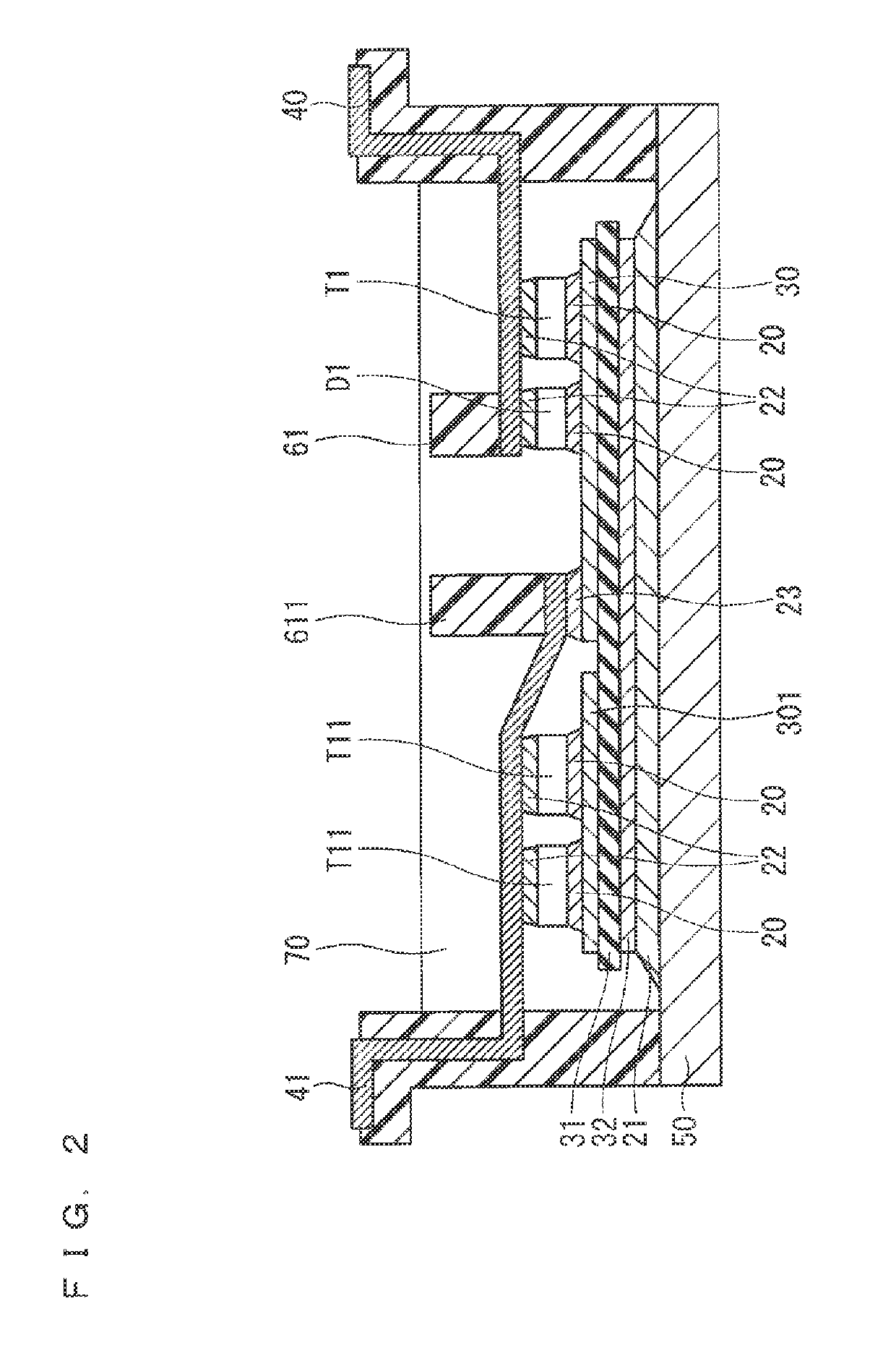
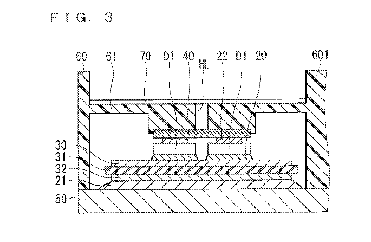
[0020]FIG. 1 is a plan view illustrating a configuration of a semiconductor device module 100 according to Embodiment 1 of the present invention. The semiconductor device module illustrated in FIG. 1 is the one that packages, as one module, power devices such as an insulated gate bipolar transistor (IGBT), a metal-oxide-semiconductor field-effect transistor (MOSFET), and a free wheeling diode (FWD). FIG. 1 illustrates a three-phase inverter as one example.
[0021]In FIG. 1, for example, circuit patterns 30 and 301 are placed on an insulating substrate 31 made of, for example, aluminum nitride (AlN), inside a resin case 60 (insulating case). Switching devices T1 and diode devices D1 are mounted on the circuit pattern 30, and switching devices T11 and diode devices D11 are mounted on the circuit pattern 301. The switching devices T1 and the diode devices D1 are each two devices connected in parallel, and the switching devices T11 and the diode devices D11 are also each two devices conne...
embodiment 2
[0070]FIG. 9 is a plan view illustrating a configuration of a semiconductor device module 200 according to Embodiment 2 of the present invention. Although the semiconductor device module illustrated in FIG. 9 is the one that packages, as one module, power devices such as an IGBT, a MOSFET, and a FWD, similarly as the semiconductor device module illustrated in FIG. 1, FIG. 9 illustrates a single-phase inverter. In FIG. 9, the same reference numerals are attached for the same structure as that of the semiconductor device module 100 described with reference to FIG. 1, and the overlapping description will be omitted.
[0071]In these days when the high-output semiconductor device modules have been sought, the number of semiconductor devices connected in parallel tends to increase, which upsizes the modules even with inclusion of the single-phase inverters.
[0072]In FIG. 9, circuit patterns 302 and 303 are placed on the insulating substrate 31. The switching devices T1 and the diode devices ...
PUM
 Abstract
Description
Claims
Application Information
 - R&D Engineer
- R&D Manager
- IP Professional
- Industry Leading Data Capabilities
- Powerful AI technology
- Patent DNA Extraction
Browse by: Latest US Patents, China's latest patents, Technical Efficacy Thesaurus, Application Domain, Technology Topic.
© 2024 PatSnap. All rights reserved.Legal|Privacy policy|Modern Slavery Act Transparency Statement|Sitemap