Semiconductor device and method for driving the same
a technology of semiconductor devices and semiconductors, applied in the direction of pulse techniques, electronic switching, emergency protective circuit arrangements, etc., can solve the problems of increasing the chip size and substrate area of the mosfet, complicated assembly, and increasing the complexity of the substrate wiring pattern, so as to reduce the size and cost of the semiconductor device
- Summary
- Abstract
- Description
- Claims
- Application Information
AI Technical Summary
Benefits of technology
Problems solved by technology
Method used
Image
Examples
first preferred embodiment
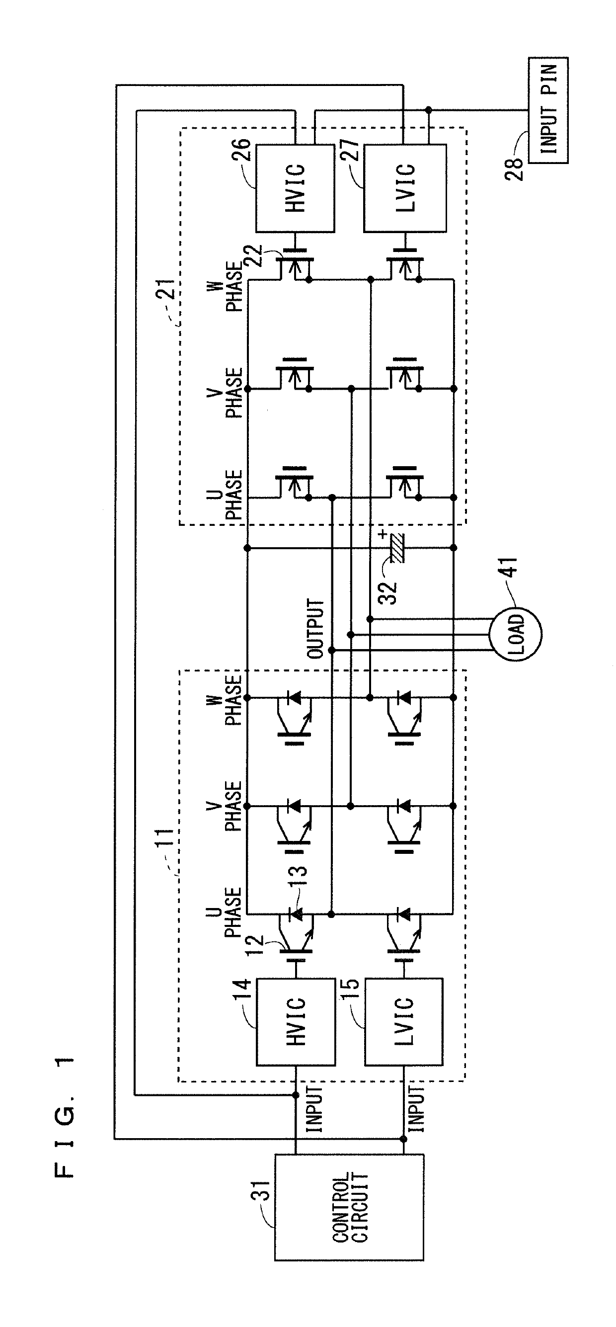
[0017]FIG. 1 is a circuit diagram illustrating the configuration of a semiconductor device according to a first preferred embodiment of the present invention. The semiconductor device in FIG. 1 includes a first power semiconductor module, which in this preferred embodiment is an insulated-gate bipolar transistor (IGBT) module 11, a second power semiconductor module, which in this preferred embodiment is a metal-oxide-semiconductor field-effect transistor (MOSFET) module 21, a control circuit 31, and an electrolytic capacitor 32.
[0018]The control circuit 31 is a microcomputer for instance, and controls the IGBT module 11 and the MOSFET module 21.
[0019]The IGBT module 11 and the MOSFET module 21 have inputs connected to the control circuit 31. The IGBT module 11 and the MOSFET module 21 have outputs connected to a load 41, such as a motor. In this way, the MOSFET module 21 according to the first preferred embodiment is connected to the IGBT module 11 in parallel between the input and ...
second preferred embodiment
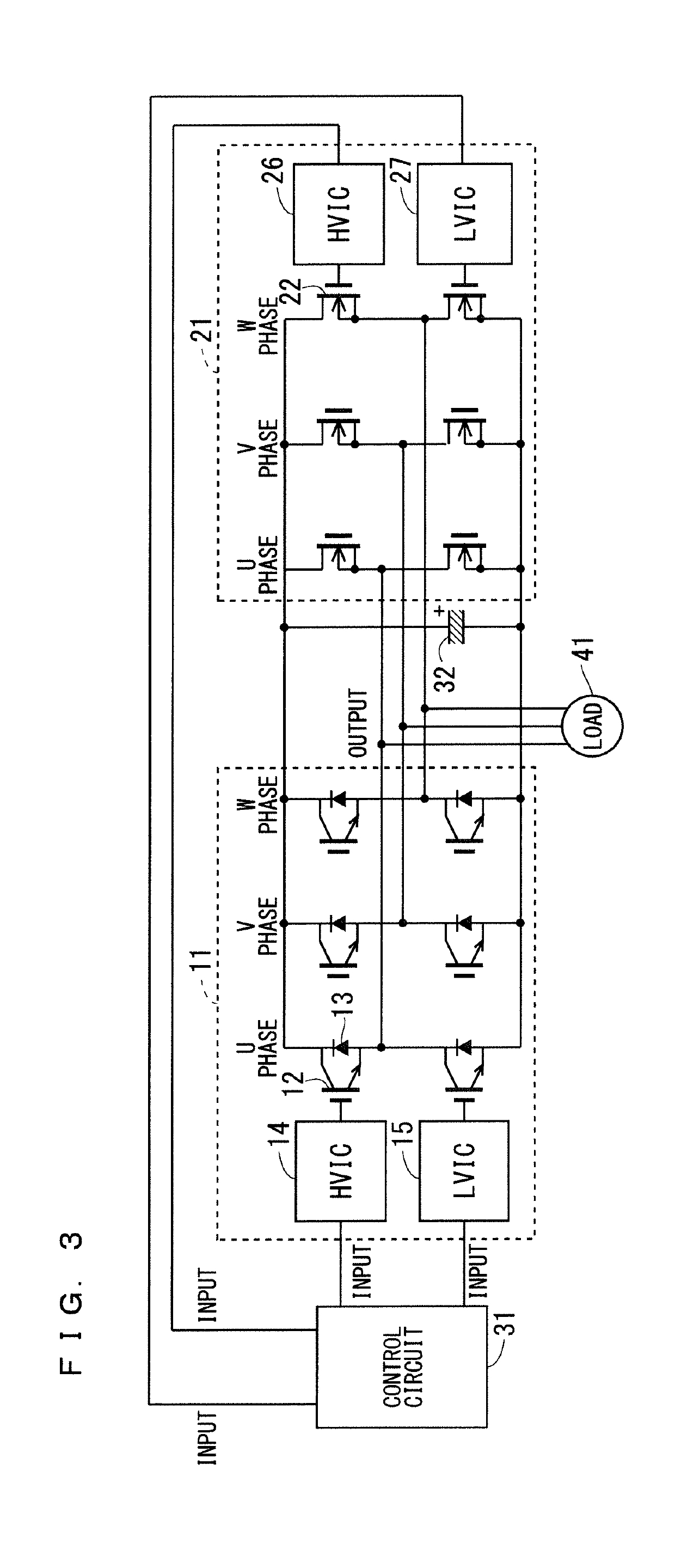
[0031]FIG. 3 is a circuit diagram illustrating the configuration of a semiconductor device according to a second preferred embodiment of the present invention. The same or similar components between the first and second preferred embodiments are denoted by the same reference signs. Thus, mainly described are components different between the preferred embodiments.
[0032]The MOSFET module 21 according to the second preferred embodiment does not include the input pin 28. Instead, the MOSFET module 21 according to the second preferred embodiment is connected to the IGBT module 11 in parallel between the control circuit 31 and the outputs of the IGBT module 11.
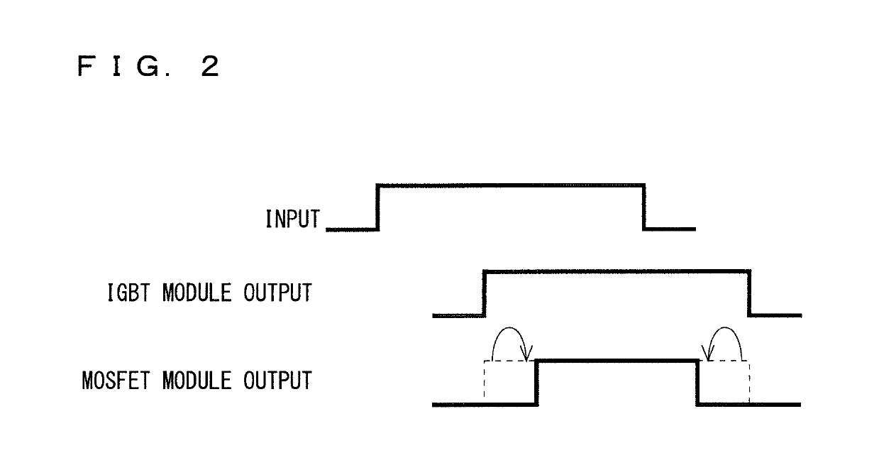
[0033]This enables the control circuit 31 to input, to the MOSFET module 21, a signal different from a signal input to the IGBT module 11. In the second preferred embodiment, the IGBT module 11 and the MOSFET module 21 can selectively execute the operation mode in response to the signal from the control circuit 31, which is describe...
third preferred embodiment
[0035]FIG. 4 is a side view of the configuration of a semiconductor device according to a third preferred embodiment of the present invention. The same or similar components between the third preferred embodiment and the first and second preferred embodiments are denoted by the same reference signs. Thus, mainly described are components different between the preferred embodiments.
[0036]The semiconductor device according to the third preferred embodiment includes a substrate 46 and a heat-dissipation fin 47 in addition to the components in the first or second preferred embodiment.
[0037]The IGBT module 11 and the MOSFET module 21 are disposed on one surface of the substrate 46. Here, the MOSFET module 21 has a switching loss of substantial zero in the configurations in the first and second preferred embodiments. In this case, the MOSFET module 21 has a relatively small package size or a relatively small rated current, have relatively little generated loss, and involves a relatively sm...
PUM
 Abstract
Description
Claims
Application Information
 - R&D
- Intellectual Property
- Life Sciences
- Materials
- Tech Scout
- Unparalleled Data Quality
- Higher Quality Content
- 60% Fewer Hallucinations
Browse by: Latest US Patents, China's latest patents, Technical Efficacy Thesaurus, Application Domain, Technology Topic, Popular Technical Reports.
© 2025 PatSnap. All rights reserved.Legal|Privacy policy|Modern Slavery Act Transparency Statement|Sitemap|About US| Contact US: help@patsnap.com


