Light irradiation type heat treatment apparatus and heat treatment method

a heat treatment apparatus and light irradiation technology, applied in the direction of optical radiation measurement, ohmic-resistance heating, instruments, etc., can solve the problems of not meeting the requirements of the joint depth, the temperature history of the semiconductor wafer in the lot becomes non-uniform, and the surface temperature of several semiconductor wafers after the first wafer, etc., to achieve accurate measurement of the effect of accurately measuring the temperature of the substra

Inactive Publication Date: 2019-05-09
DAINIPPON SCREEN MTG CO LTD
View PDF0 Cites 6 Cited by
  • Summary
  • Abstract
  • Description
  • Claims
  • Application Information

AI Technical Summary

Benefits of technology

[0017]The temperature measurement with the substrate temperature measuring part is corrected based on the temperature of the structure provided in the chamber. Thus, the method is capable of accurately measuring the temperature of the substrate irrespective of the temperature of the structure.
[0018]It is therefore an object of the present invention to accurately measure the temperature of a substrate.

Problems solved by technology

This results in a junction depth much greater than a required depth, which might constitute a hindrance to good device formation.
Thus, there arises a problem that the temperature history of the semiconductor wafers in the lot becomes non-uniform.
In particular, there is a danger that the attained surface temperature of several semiconductor wafers subsequent to the first wafer in the lot at the time of the flash irradiation does not reach a target temperature because these semiconductor wafers are supported by the susceptor that is at a relatively low temperature.
Unfortunately, such dummy running not only consumes the dummy wafers irrelevant to the treatment but also requires a considerable amount of time for the flash heating treatment of the approximately ten dummy wafers.
Thus, the dummy running presents a problem that the efficient operation of the flash lamp annealer is hindered.

Method used


Image

  • Light irradiation type heat treatment apparatus and heat treatment method
  • Light irradiation type heat treatment apparatus and heat treatment method
  • Light irradiation type heat treatment apparatus and heat treatment method

Examples


Embodiment Construction

[0028]A preferred embodiment according to the present invention will now be described in detail with reference to the drawings.

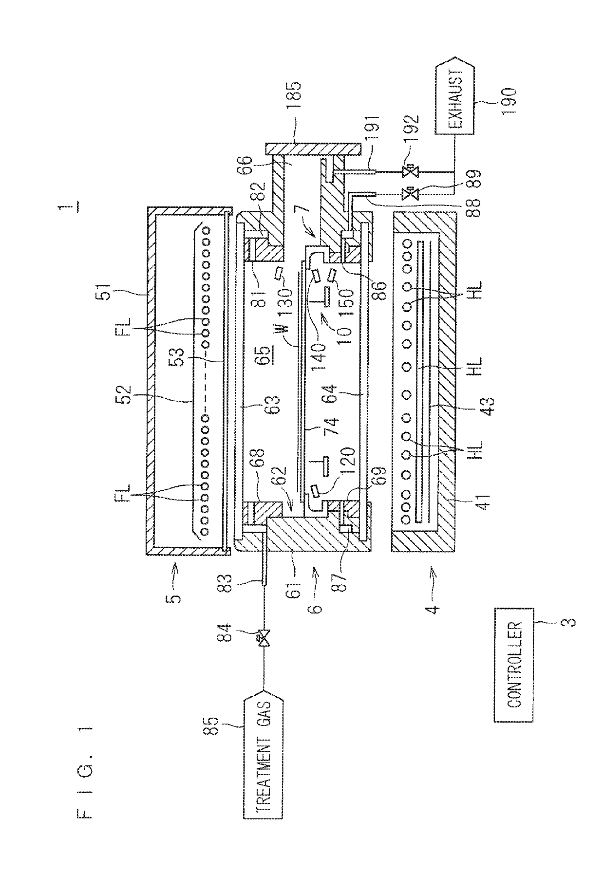
[0029]FIG. 1 is a longitudinal sectional view showing a configuration of a heat treatment apparatus 1 according to the present invention. The heat treatment apparatus 1 according to the present preferred embodiment is a flash lamp annealer for irradiating a disk-shaped semiconductor wafer W serving as a substrate with flashes of light to heat the semiconductor wafer W. The size of the semiconductor wafer W to be treated is not particularly limited. For example, the semiconductor wafer W to be treated has a diameter of 300 mm and 450 mm The semiconductor wafer W prior to the transport into the heat treatment apparatus 1 is implanted with impurities. The heat treatment apparatus 1 performs a heating treatment on the semiconductor wafer W to thereby activate the impurities implanted in the semiconductor wafer W. It should be noted that the dimensions of compone...


PUM


Abstract

A semiconductor wafer held in a chamber by a susceptor is heated by irradiating the semiconductor wafer with light directed through an upper chamber window and a lower chamber window. A radiation thermometer measures the temperature of the semiconductor wafer held by the susceptor. A temperature correction part corrects temperature measurement of the semiconductor wafer with the radiation thermometer, based on the value of temperature measurement of the upper chamber window, the value of temperature measurement of the lower chamber window, and the value of temperature measurement of the susceptor. Thus, the temperature of the semiconductor wafer is accurately measured irrespective of the temperatures of in-chamber structures including the susceptor and the like.

Description

BACKGROUND OF THE INVENTIONField of the Invention[0001]The present invention relates to a heat treatment apparatus and a heat treatment method which irradiate a thin plate-like precision electronic substrate (hereinafter referred to simply as a “substrate”) such as a semiconductor wafer with light to heat the substrate.Description of the Background Art[0002]In the process of manufacturing a semiconductor device, impurity doping is an essential step for forming a pn junction in a semiconductor wafer. At present, it is common practice to perform impurity doping by an ion implantation process and a subsequent annealing process. The ion implantation process is a technique for causing ions of impurity elements such as boron (B), arsenic (As) and phosphorus (P) to collide against the semiconductor wafer with high acceleration voltage, thereby physically implanting the impurities into the semiconductor wafer. The implanted impurities are activated by the subsequent annealing process. When ...

Claims


Application Information

Patent Timeline
Patent Type & Authority Applications(United States)
IPC IPC(8): H05B3/00G01J5/00H01L21/67H01L21/324
CPCH05B3/0047G01J5/0096H01L21/67115H01L21/324G01J2005/0048G01J5/10H01L21/6719H01L21/67248H01L21/6875H01L21/67098H01L21/683G01J5/80
Inventor ITO, YOSHIO
Owner DAINIPPON SCREEN MTG CO LTD
Why Eureka
Try Eureka