Liquid crystal device and electronic apparatus

Inactive Publication Date: 2019-07-18
SEIKO EPSON CORP
View PDF13 Cites 1 Cited by
  • Summary
  • Abstract
  • Description
  • Claims
  • Application Information

AI Technical Summary

Benefits of technology

[0005]In view of the above, the object of the invention is to provide a liquid crystal device capable of suppressing t

Problems solved by technology

However, a defective alignment of the liquid crystal (reverse tilt domain) occurs due to an influence of a lateral electric field generated between pixel electrodes adjacent to each other when the pixel pitch is narrowed to achieve a downsizing and a high definition, which may readily cau

Method used


Image

  • Liquid crystal device and electronic apparatus
  • Liquid crystal device and electronic apparatus
  • Liquid crystal device and electronic apparatus

Examples


exemplary embodiment 1

Configuration of Liquid Crystal Device

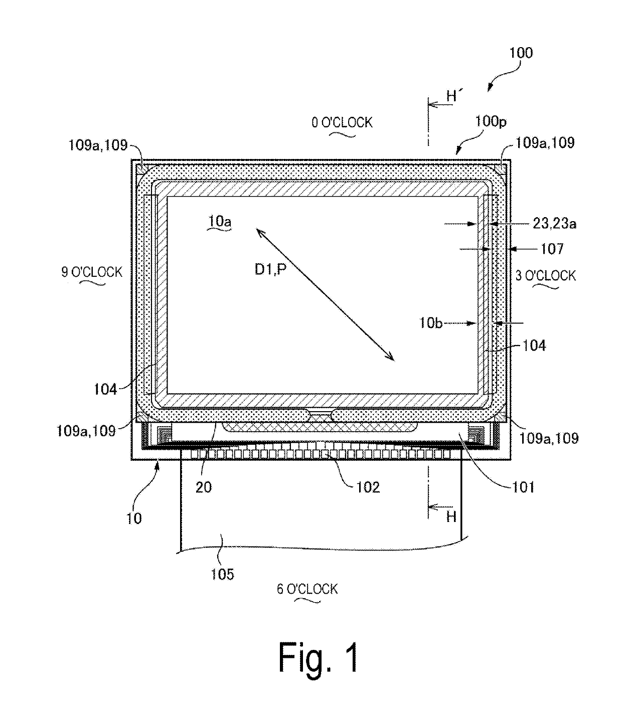
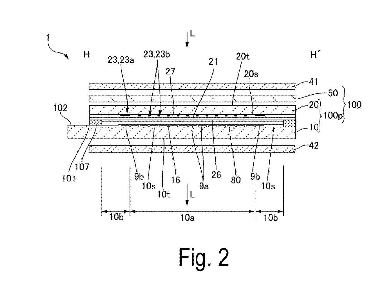
[0030]FIG. 1 is a plan view illustrating one aspect of a liquid crystal device 100 according to Exemplary Embodiment 1 of the invention. FIG. 1 illustrates a state where the liquid crystal device 100 is viewed from the side of a second substrate 20. FIG. 2 is an H-H′ cross-sectional view of the liquid crystal device 100 illustrated in FIG. 1. Note that, in FIG. 1, a liquid crystal panel 100p alone is illustrated while omitting the illustration of an optical compensation element 50 illustrated in FIG. 2.

[0031]As illustrated in FIG. 1 and FIG. 2, the liquid crystal device 100 includes the liquid crystal panel 100p in which a first substrate 10 having light translucency and the second substrate 20 having light translucency are bonded together with a sealing material 107 creating a predefined gap in between, and the optical compensation element 50. The optical compensation element 50, which also serves as a phase difference compensation element, is ...

exemplary embodiment 2

[0067]FIG. 9 is an explanatory diagram illustrating the image processing circuit 130 (image processing device) of the light modulation apparatus 1 according to Exemplary Embodiment 2 of the invention. FIGS. 10A to 10C are explanatory diagrams illustrating a correction of an applied voltage performed by the image processing circuit illustrated in FIG. 9. FIG. 11 is an explanatory diagram illustrating a detection of a boundary by the image processing circuit 130 illustrated in FIG. 9. Note that the light modulation device 1 of Exemplary Embodiment 1 includes the configuration of the image processing circuit 130 replaced by the aspect illustrated in FIG. 9 in the light modulation device 1 according to Exemplary Embodiment 1. Accordingly, common components are referenced using like numbers, and no descriptions for such components are provided below.

[0068]In Exemplary Embodiment 2, the image processing circuit 130 illustrated in FIG. 9, in a case when a pixel (first pixel) of an applied ...

exemplary embodiment 3

[0077]FIG. 12 is an explanatory diagram illustrating a grayscale voltage and the like of the liquid crystal device 100 according to Exemplary Embodiment 3 of the invention. Although Exemplary Embodiments 1 and 2 employ a normally black mode, the invention may also be applied when a normally white mode is employed. In this case, the grayscale voltage and the like are as illustrated in FIG. 12, where only black and white are interchanged with reference to Exemplary Embodiments 1 and 2. Thus, the corresponding voltages and the like are referenced using like numbers in FIG. 8 and FIG. 11, and no descriptions for such elements are provided below. That is, the optical compensation element is disposed such that, in the light intensity-voltage characteristic, the intensity of the light emitted from the liquid crystal element is maximized with an applied voltage Vwt corresponding to a point belonging to an area having a large change in inclination of a tangent line disposed between two areas...


PUM


Abstract

A transmissive-type liquid crystal device of a normally black mode, an image processing circuit configured to output an applied voltage to be applied to a liquid crystal element, and a phase difference compensation element configured to cancel a phase difference occurring inside of the liquid crystal element. The phase difference compensation element is disposed such that, in relative transmittance-voltage characteristics representing a relationship between an applied voltage and an intensity of light emitted from the liquid crystal element, the intensity of the light emitted from the liquid crystal element is minimized with an applied voltage corresponding to a point belonging to an area Z having a large change in inclination of a tangent line disposed between areas X and Y exhibiting a small change in inclination of a tangent line touching each of points on a light intensity-voltage characteristic corresponding to each of applied voltages at every predefined voltage interval.

Description

BACKGROUND1. Technical Field[0001]The invention relates to a liquid crystal device in which an optical compensation element is provided in a liquid crystal panel, and an electronic apparatus.2. Related Art[0002]A liquid crystal panel includes a liquid crystal layer between a plurality of pixel electrodes formed on a first substrate and a common electrode formed on a second substrate. The liquid crystal panel configures a liquid crystal device together with an optical compensation element disposed on at least one of the opposite side to the second substrate with respect to the first substrate and the opposite side to the first substrate with respect to the second substrate. In such a liquid crystal device, a voltage corresponding to a grayscale level of each of the pixels is applied between the pixel electrode and the common electrode, then an alignment state of the liquid crystal molecules is defined for each pixel in the liquid crystal layer, and in this state the transmittance or ...

Claims


Application Information

Patent Timeline
IPC IPC(8): G02F1/137G02F1/13363G09G3/36
CPCG02F1/137G02F1/13363G09G3/3607G02F2203/01G02F2203/64G02F2203/30G02F2001/13712G02F1/133734G02F1/133528G02F2001/133531G03B21/006G09G3/3648G09G2320/0261G09G2360/16G02F1/13712G02F1/133531
Inventor AOKI, TORU
Owner SEIKO EPSON CORP
Why Eureka
Try Eureka