Antenna structure and electronic device comprising antenna structure

a technology of electronic devices and antennas, applied in the direction of individual energised antenna arrays, polarised antenna unit combinations, particular array feeding systems, etc., can solve the problems of distortion of pattern, inefficient use of conventional methods, small size and/or weight of antennas and devices, etc., and achieve the effect of efficient mounting

Active Publication Date: 2019-07-25
SAMSUNG ELECTRONICS CO LTD
View PDF0 Cites 21 Cited by
  • Summary
  • Abstract
  • Description
  • Claims
  • Application Information

AI Technical Summary

Benefits of technology

[0011]According to various example embodiments of the present disclosure, a plurality of antennas may be efficiently mounted in a small space defined within an electronic device.
[0012]According to various example embodiments of the present disclosure, distortion of a beam pattern or a radiation pattern due to a housing of the electronic device may be effectively prevented.

Problems solved by technology

If the ultra-high-band frequency is used, a wavelength may become short, and thus, an antenna and a device may become small-sized and / or lightweight.
In this case, a beam pattern or a radiation pattern formed by the antenna may have an influence of a housing, thereby causing distortion of the pattern.
However, since a large number of feed lines for supplying a power are required in the case of an antenna array, it may be inefficient to use the conventional way due to a limitation on a mounting space in the electronic device.

Method used


Image

  • Antenna structure and electronic device comprising antenna structure
  • Antenna structure and electronic device comprising antenna structure
  • Antenna structure and electronic device comprising antenna structure

Examples


Embodiment Construction

[0037]Hereinafter, various example embodiments of the present disclosure will be described with reference to accompanying drawings. However, those of ordinary skill in the art will recognize that various modifications, equivalents, and / or alternatives of the various example embodiments described herein can be variously made without departing from the scope and spirit of the present disclosure.

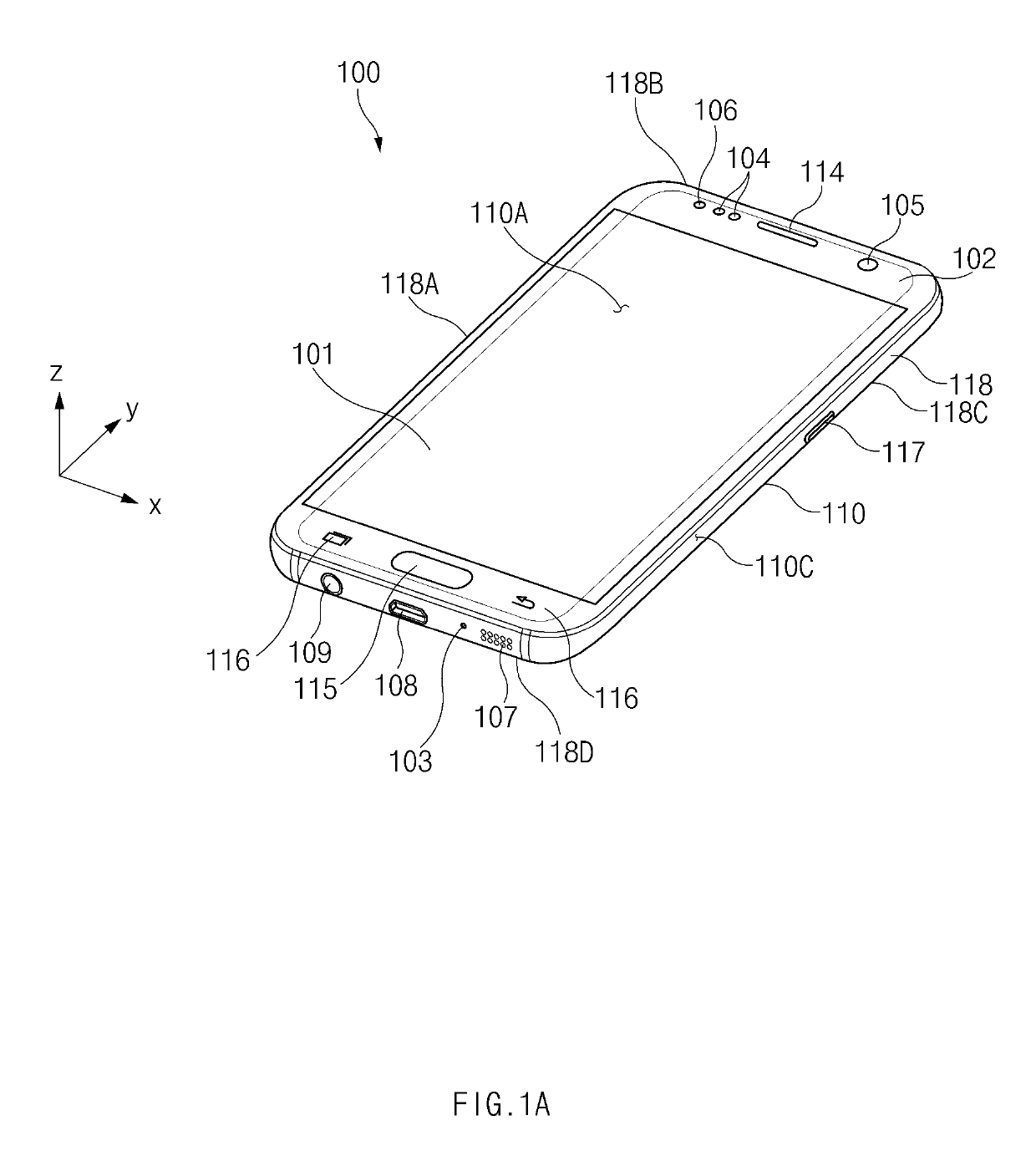
[0038]FIG. 1A is a front perspective view illustrating a mobile electronic device according to an embodiment.

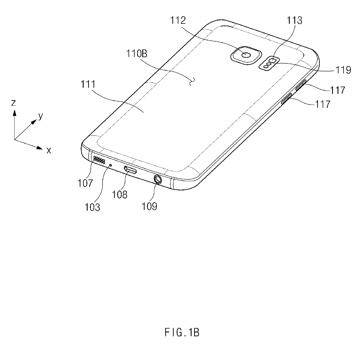
[0039]FIG. 1B is a back perspective view illustrating an electronic device of FIG. 1A.

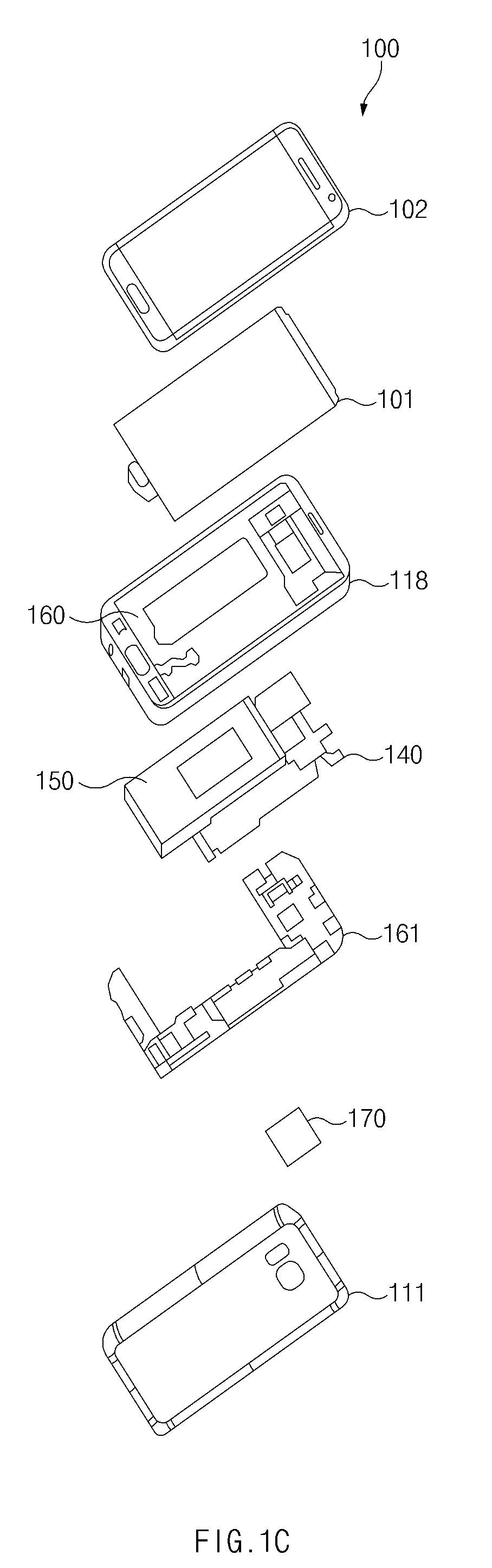
[0040]Referring to FIGS. 1A and 1B, an electronic device 100 according to an embodiment may include a housing 110 including a first surface (or a front surface) 110A, a second surface (or a back surface) 110B, and a side surface 110C surrounding a space between the first surface 110A and the second surface 110B. In another embodiment (not illustrated), the housing 110 may refer to a structure which form...


PUM


Abstract

An electronic device includes a housing that includes a first plate, a second plate facing a direction opposite the first plate, and a side member surrounding a space between the first plate and the second plate, an antenna structure that includes a plurality of dielectric layers perpendicular to the side member and parallel to the first plate, a first array of conductive plates aligned in a first direction perpendicular to the first plate at a first dielectric layer of the dielectric layers, a second array of conductive plates spaced from the first array and aligned in the first direction at the first dielectric layer, wherein the second array is farther from the first plate than the first array, at least one ground plane positioned on at least one of the dielectric layers and interposed between the first array and the second array, when viewed from above the side member, and a wireless communication circuit electrically connected to the first array and the second array and configured to transmit and / or receive a signal having a frequency in a range of 20 GHz to 100 GHz.

Description

CROSS-REFERENCE TO RELATED APPLICATION[0001]This application is based on and claims priority under 35 U.S.C. § 119 to Korean Patent Application No. 10-2018-0008995, filed on Jan. 24, 2018, in the Korean Intellectual Property Office, the disclosure of which is incorporated by reference herein its entirety.BACKGROUND1. Field[0002]The disclosure relates to an antenna structure and an electronic device including the antenna structure.2. Description of Related Art[0003]As the mobile traffic sharply increases, a 5th generation (5G) mobile communication technology based on an ultra-high-band frequency of 20 GHz or higher is being developed. A signal of the ultra-high-band frequency includes a millimeter wave (mmWave) having a frequency band ranging from 20 GHz to 100 GHz. If the ultra-high-band frequency is used, a wavelength may become short, and thus, an antenna and a device may become small-sized and / or lightweight. Also, the short wavelength may enable mounting relatively many antennas...

Claims


Application Information

Patent Timeline
Patent Type & Authority Applications(United States)
IPC IPC(8): H01Q1/42H01Q1/38H01Q19/13H01Q21/00H01Q11/14H01Q1/52
CPCH01Q1/422H01Q1/38H01Q19/138H01Q21/0031H01Q11/14H01Q1/523H01Q21/062H01Q1/243H01Q21/28H01Q21/08H01Q21/24H01Q9/0485H01Q9/285H01Q1/50H04M1/0202
Inventor JONG, JE HUNPARK, SE HYUNYUN, SU MINJEONG, MYUNG HUNJO, JAE HOONJUNG, JIN WOOCHUN, JAE BONG
Owner SAMSUNG ELECTRONICS CO LTD
Why Eureka
Try Eureka