Organic light emitting display device

a light-emitting display and organic technology, applied in the direction of semiconductor devices, basic electric elements, electrical apparatus, etc., can solve the problems of contact hole profile failure, and achieve the effects of reducing manufacturing costs, increasing reliability, and increasing the interface characteristics of the second active layer

Active Publication Date: 2019-08-15
SAMSUNG DISPLAY CO LTD
View PDF3 Cites 2 Cited by
  • Summary
  • Abstract
  • Description
  • Claims
  • Application Information

AI Technical Summary

Benefits of technology

[0027]In addition, as the third insulation layer and the protective insulation layer, which consist essentially of SiOx, are in direct contact with the second active layer, interface characteristics of the second active layer may be relatively increased. Accordingly, the OLED device according to example embodiments may include the second semiconductor element where reliability is increased.
[0028]In a method of manufacturing the OLED device according to example embodiments, a heat treatment process is performed on the first active layer and the second active layer. When the heat treatment process is performed, a driving-range of a first semiconductor element that corresponds to a driving transistor may be relatively widened, and the second semiconductor element that is relatively precise may be obtained because a scattering of a threshold voltage of a second semiconductor element that corresponds to a switching transistor is reduced. In addition, as the heat treatment process is simultaneously performed on the first active layer and the second active layer, a manufacturing cost of the OLED device may be relatively decreased.

Problems solved by technology

An under cut phenomenon may occur in an insulation layer located in the contact hole by the etchant of the BOE process, and a profile failure of the contact hole may be generated.

Method used


Image

  • Organic light emitting display device
  • Organic light emitting display device
  • Organic light emitting display device

Examples


Embodiment Construction

[0035]Hereinafter, embodiments of the present inventive concept will be explained in detail with reference to the accompanying drawings.

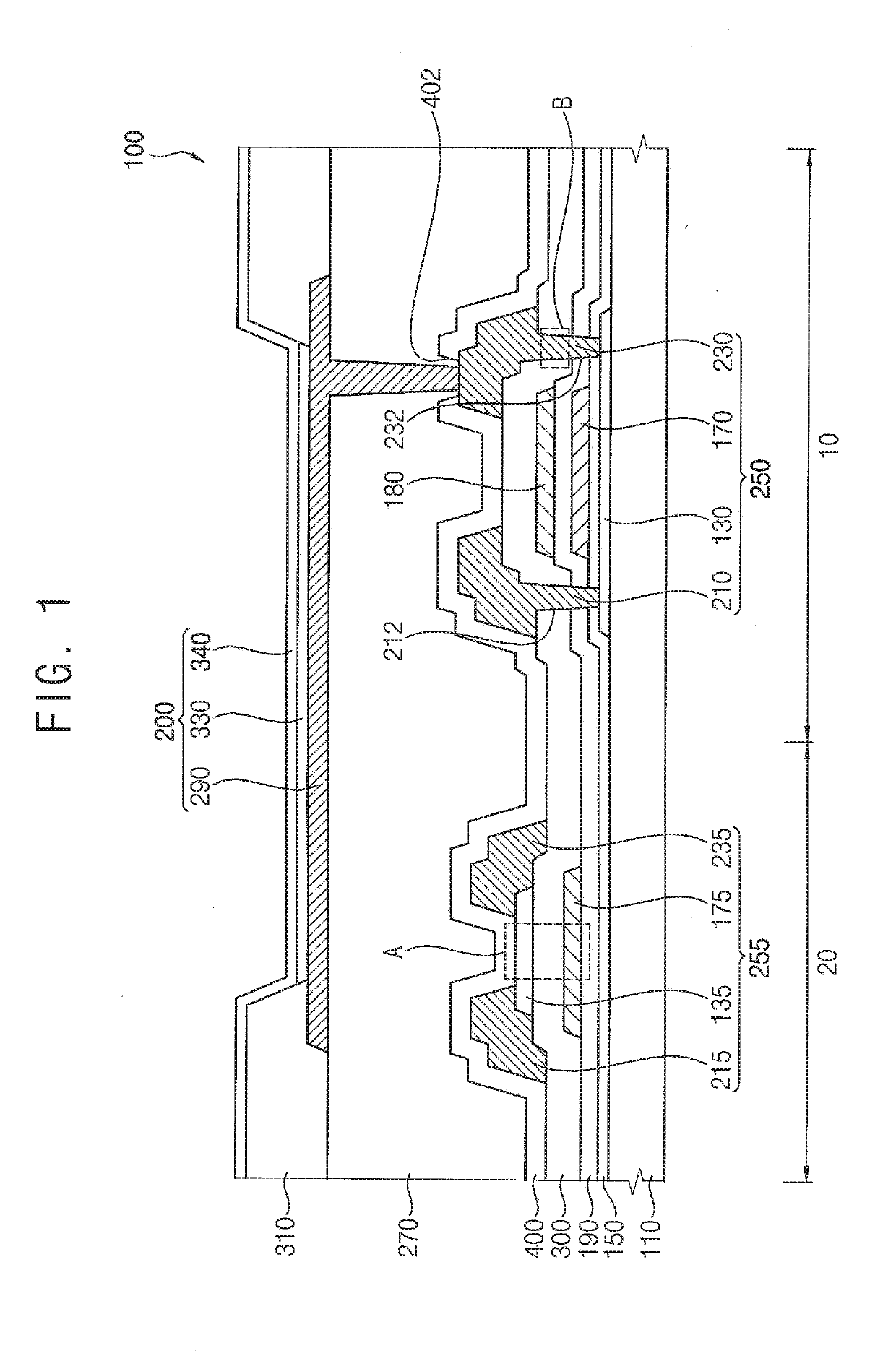
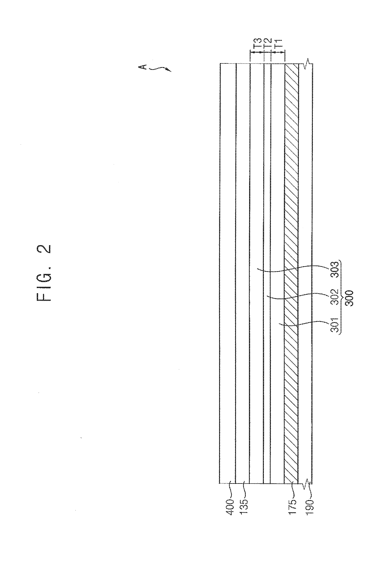
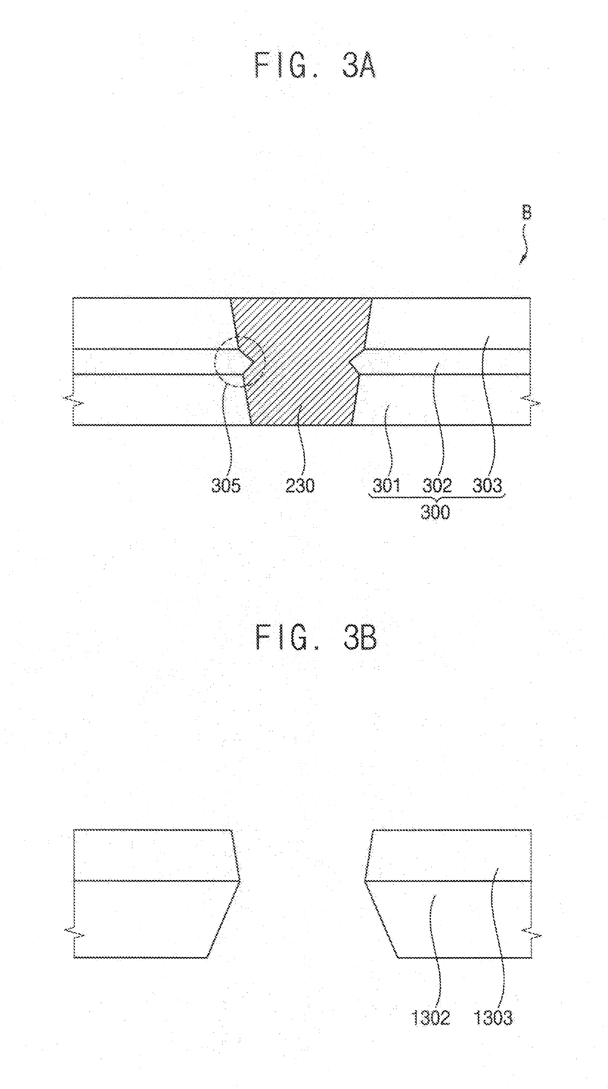
[0036]FIG. 1 is a cross-sectional view illustrating an organic light emitting display (OLED) device 100 in accordance with example embodiments. FIG. 2 is an enlarged cross-sectional view corresponding to region ‘A’ of FIG. 1. FIG. 3A is an enlarged cross-sectional view corresponding to region ‘B’ of FIG. 1. FIG. 3B is an enlarged cross-sectional view for describing an under-cut phenomenon.

[0037]Referring to FIGS. 1, 2 and 3A, the OLED device 100 may include a substrate 110, a first semiconductor element 250, a second semiconductor element 255, a gate electrode pattern 180, a gate insulation layer 150, an insulating interlayer 190, an insulation layer structure 300, a protective insulation layer 400, a planarization layer 270, a light emitting structure 200, a pixel defining layer 310, etc. Here, the first semiconductor element 250 may include a firs...


PUM


Abstract

An organic light emitting display device includes a substrate, a first semiconductor element, a second semiconductor element, an insulation layer structure, and a light emitting structure. The substrate has a first region and a second region that is adjacent to the first region. The insulation layer structure is disposed between a second gate electrode and a second active layer of the second semiconductor element. The insulation layer structure includes a first insulation layer having a first etching rate, a second insulation layer disposed on the first insulation layer and having a second etching rate that is greater than the first etching rate, and a third insulation layer disposed on the second insulation layer and having a third etching rate that is less than the second etching rate in a same etching process. The light emitting structure is disposed on the insulation layer structure.

Description

CROSS-REFERENCE TO RELATED APPLICATION(S)[0001]This application claims priority under 35 USC § 119 to Korean Patent Applications No. 10-2018-0017149, filed on Feb. 12, 2018 in the Korean Intellectual Property Office (KIPO), the contents of which are incorporated herein in its entirety by reference.BACKGROUND1. Field[0002]Example embodiments relate generally to an organic light emitting display device. More particularly, embodiments of the present inventive concept relate to an organic light emitting display device including an insulation layer structure.2. Description of the Related Art[0003]A flat panel display (FPD) device is widely used as a display device of an electronic device because the FPD device is lightweight and thin compared to a cathode-ray tube (CRT) display device. Typical examples of the FPD device are a liquid crystal display (LCD) device and an organic light emitting display (OLED) device.[0004]Recently, the OLED device that simultaneously (or concurrently) includ...

Claims


Application Information

Patent Timeline
Patent Type & Authority Applications(United States)
IPC IPC(8): H01L27/32
CPCH01L27/3262H01L27/3258H01L27/3246H01L27/3248H01L27/1251H10K59/124H10K59/131H01L27/124H01L27/1225H10K59/1213H10K59/123H10K71/231H10K50/84H10K59/122
Inventor SON, KYOUNG SEOKKIM, JAYBUMMOON, YEON KEONLIM, JUN HYUNG
Owner SAMSUNG DISPLAY CO LTD
Why Eureka
Try Eureka