Organic Electroluminescent Device And Manufacturing Method Therefor

a technology of electroluminescent devices and manufacturing methods, applied in the direction of semiconductor devices, basic electric elements, electrical apparatus, etc., can solve the problems of high equipment investment and process costs, low material utilization rate, and high probability, and achieve the effects of enhancing characteristics, reducing the deterioration of charge characteristics by residual organic materials, and improving interface characteristics with electrodes

Pending Publication Date: 2019-05-23
LG CHEM LTD
View PDF8 Cites 1 Cited by
  • Summary
  • Abstract
  • Description
  • Claims
  • Application Information

AI Technical Summary

Benefits of technology

[0023]In the present specification, a Group V, Group VI or Group VII transition metal may be doped or mixed with one or more of Group I, Group VIII, Group XI, and Group XII metals as described above in order to form a hole injection or transporting layer or a charge generating layer of an organic electroluminescent device, thereby diversifying charge injection characteristics by varying a work function of a layer to be formed by using the doped or mixed metals.
[0024]Further, the present specification may provide a coating composition including a Group V, Group VI, or Group VII transition metal, an organic metal complex or metal salt including Group I, Group VIII, Group XI, and Group XII metal, and an organic solvent as described above in order to form a hole injection or transporting layer or a charge generating layer of an organic electroluminescent device, and may provide an organic electroluminescent device whose characteristics are enhanced because an electrode such as an ITO electrode is not damaged by using the coating composition, interface characteristics with the electrode are improved, and resistance to a solvent used for an upper layer such as a hole transporting layer or a light emitting layer is excellent.
[0025]In the case of a hole injection or transporting layer or a charge generating layer obtained from the ink composition, the solvent is removed during a drying process after the coating, and an organic material ligand of an organic metal complex is decomposed by reacting with oxygen in the air and thus removed during a heat treatment process, and the layer is present in the form of a finally doped metal oxide, and as a result, a deterioration in charge characteristics by the residual organic material is minimized, and particularly, an organic light emitting device having a long service life may be obtained. Further, when the ligand is oxidized while being decomposed during the heat treatment process of the coating film, the central metal element is reacted with oxygen in the air to generate a M-O-M bond, and as a result, MO3, for example, a form of MoO3 or WO3 and V2O5 is produced, and simultaneously, another type of oxide such as W2O5 or Mo2O5 may be partially produced due to a M-M bond in which metal atoms are bonded to each other in some parts, thereby imparting doping effects of the metal oxide caused by oxygen deficiency known as the doping mechanism of the general metal oxide. As a result, in the case of a hole injection layer formed of vacuum deposited MoO3 or WO3, and the like, the driving voltage is sharply increased while the thickness is increased, and unlike the hole injection layer almost acting as an insulator, particularly, when the thickness is 30 nm or more, a hole injection or transporting layer or a charge generating layer, which is composed of a metal oxide and prepared by using the ink composition according to the present specification, has an increase in charge concentration and charge mobility in the entire metal oxide thin film due to the aforementioned doping effects, and thus provides a characteristic in which an increase in driving voltage does not occur even when the thickness is increased to 30 nm or more.
[0026]Further, during the heat treatment process after the coating, the metal in the organic metal complex is bonded to an oxygen atom present at the interface of the ITO while the bond between the metal in the organic metal complex and the organic material ligand is broken, and as a result, the interface between an anode and a metal oxide thin film being a hole injection layer is improved while the bond such as the Metal-O—In or Metal-O—Sn is produced, so that unlike the deposited thin film, the mechanical strength of the thin film is increased, the interface characteristics are improved, and as a result, the charge may smoothly move between the anode and the metal oxide thin film.
[0027]In addition, by using the organic solvent as described above, the thin film formation characteristics after the coating are excellent, a mass production process of an inkjet, and the like is enabled, and device characteristics may be improved by eliminating residual moisture, as compared to the case of using an aqueous solution obtained by adding and dissolving a metal oxide powder such as MoO3 or V2O5 itself into H2O2 or NH4OH, and the like. In particular, according to exemplary embodiments of the present specification, by using the above-described organic metal complex even though a substituent such as a halogen group is partially included, it is possible to prepare an ink which is substituted with a solvent and thus has an appropriate viscosity and good coatability while being dissolved in ketone and an alcohol-based or ester-based solvent, and it is possible to advantageously manufacture a hole injection or transporting layer or a charge generating layer by a coating method using the ink.

Problems solved by technology

When an organic electroluminescent device is manufactured by using a vacuum process, there are disadvantages in that equipment investment costs and process costs are high, there is a limitation in uniformly making the organic electroluminescent device have a large area, and the material utilization rate is low due to the high ratio of material discarded without being deposited onto a substrate during the deposition.
However, when layers constituting an organic electroluminescent device are stacked through a solution process unlike a deposition process, it is highly likely that a lower layer may be damaged by a process of forming an upper layer.
That is, there may occur a phenomenon in which a material in the lower layer is dissolved again by a solvent or ink used in the solution process, and thus is mixed with the upper layer, or a thin film is physically damaged.
However, these conductive polymers are usually characterized by damaging an electrode material being a lower layer by using an acidic dopant material with a low pH, and have a disadvantage in that service life characteristics deteriorate due to the characteristic.
However, this method still has a resistance problem with a solvent or ink of a post-process as previously mentioned.

Method used


Image

  • Organic Electroluminescent Device And Manufacturing Method Therefor
  • Organic Electroluminescent Device And Manufacturing Method Therefor
  • Organic Electroluminescent Device And Manufacturing Method Therefor

Examples


example 1

[0121]A solution in which copper acetate and Mo(CO)6 at a weight ratio of 0.8:99.2 were dissolved at a concentration of 4 wt % in cyclohexanone was prepared. A glass substrate coated with ITO was washed sequentially with water and isopropanol, and then the mixed solution was spin-coated onto an ITO-deposited base material at 1,000 rpm for 30 seconds. The obtained thin film was subjected to heat treatment under an oxygen atmosphere at 200° C. for 15 minutes, thereby forming a hole injection layer having a very uniform thickness of 30 nm.

[0122]A hole transporting layer having a thickness of 45 nm was formed on the top of the hole injection layer by using 4,4′-bis[N-(1-naphthyl)-N-phenylamino]biphenyl (NPB).

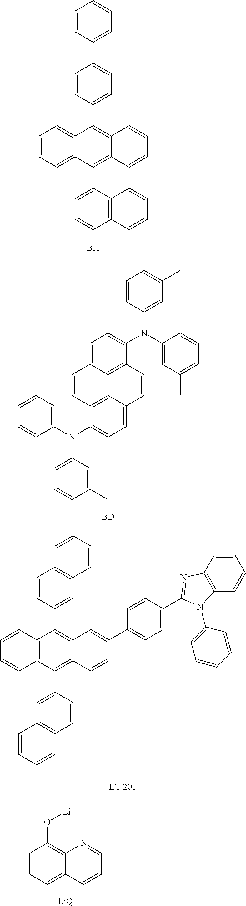
[0123]An electron blocking layer was formed to have a thickness of 15 nm on the top of the hole transporting layer. BH of the following chemical formula being a blue fluorescent host was doped with BD being a blue dopant at a weight ratio of 95:5 on the electron blocking layer, ther...

example 2

[0126]A device was manufactured in the same manner as in Example 1, except that NaNO3 and MoO2(acac)2 at a weight ratio of 5:95 were dissolved at a concentration of 4 wt % in ethylene glycol monomethyl ether, the resulting solution was coated at 1,000 rpm on an ITO-deposited base material, and then a heat treatment was carried out under an oxygen atmosphere, thereby preparing a hole injection layer. At this time, the thickness of the hole injection layer was 30 nm. Characteristics of the device are shown in Table 1.

example 3

[0127]A device was manufactured in the same manner as in Example 1, except that AgNO3 and MoO2(acac)2 at a weight ratio of 0.5:99.5 were dissolved at a concentration of 4 wt % in ethylene glycol monomethyl ether, the resulting solution was coated at 1,000 rpm on an ITO-deposited base material, and then a heat treatment was carried out under an oxygen atmosphere, thereby preparing a hole injection layer. At this time, the thickness of the hole injection layer was 30 nm. Characteristics of the device are shown in Table 1.


PUM


Abstract

The present specification relates to a coating composition for a hole injection or transporting layer or a charge generating layer of an organic electroluminescent device, the coating composition including: an organic metal complex including one or more of Group V, Group VI, and Group VII transition metals; an organic metal complex or metal salt including one or more of Group I, Group VIII, Group XI, and Group XII metals; and an organic solvent, and a method for manufacturing an organic electroluminescent device and an organic electroluminescent device using the same.

Description

TECHNICAL FIELD[0001]The present specification claims priority to and the benefit of Korean Patent Application No. 10-2016-0057050 filed in the Korean Intellectual Property Office on May 10, 2016, the entire contents of which are incorporated herein by reference.[0002]The present specification relates to a method for manufacturing an organic electroluminescent device and an organic electroluminescent device manufactured by the same.BACKGROUND ART[0003]An organic light emission phenomenon is one of the examples of converting an electric current into visible rays through an internal process of a specific organic molecule. The principle of the organic light emission phenomenon is as follows. When an organic material layer is disposed between an anode and a cathode, if an electric current is applied between the two electrodes, electrons and holes are injected into the organic material layer from the cathode and the anode, respectively. The electrons and the holes which are injected into...

Claims


Application Information

Patent Timeline
Patent Type & Authority Applications(United States)
IPC IPC(8): H01L51/00
CPCH01L51/0091H01L51/0077H01L51/5088H01L51/5056H01L51/56H01L51/0007H01L51/0028H10K71/15H10K71/12H10K85/30H10K85/351H10K85/371H10K50/155H10K50/17H10K50/19H10K71/40H10K85/344H10K2102/361H10K2102/351H10K71/00H10K50/00H10K99/00H10K50/15H10K71/441
Inventor YOON, SEOKHEELEE, DONGGUKIM, HWAKYUNGJEONG, JAE HAKSHIN, JIYEONKIM, DAEHOBAE, JAESOONLEE, JAECHOL
Owner LG CHEM LTD
Why Eureka
Try Eureka