

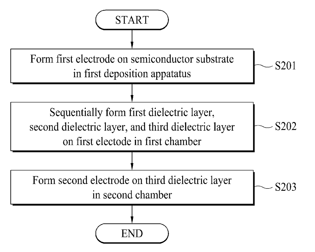
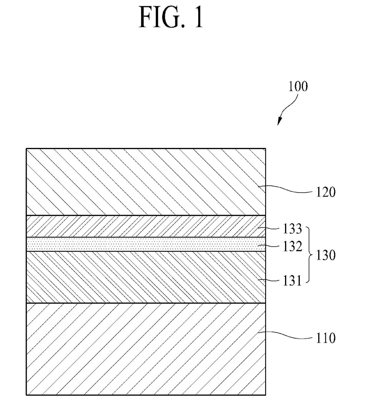
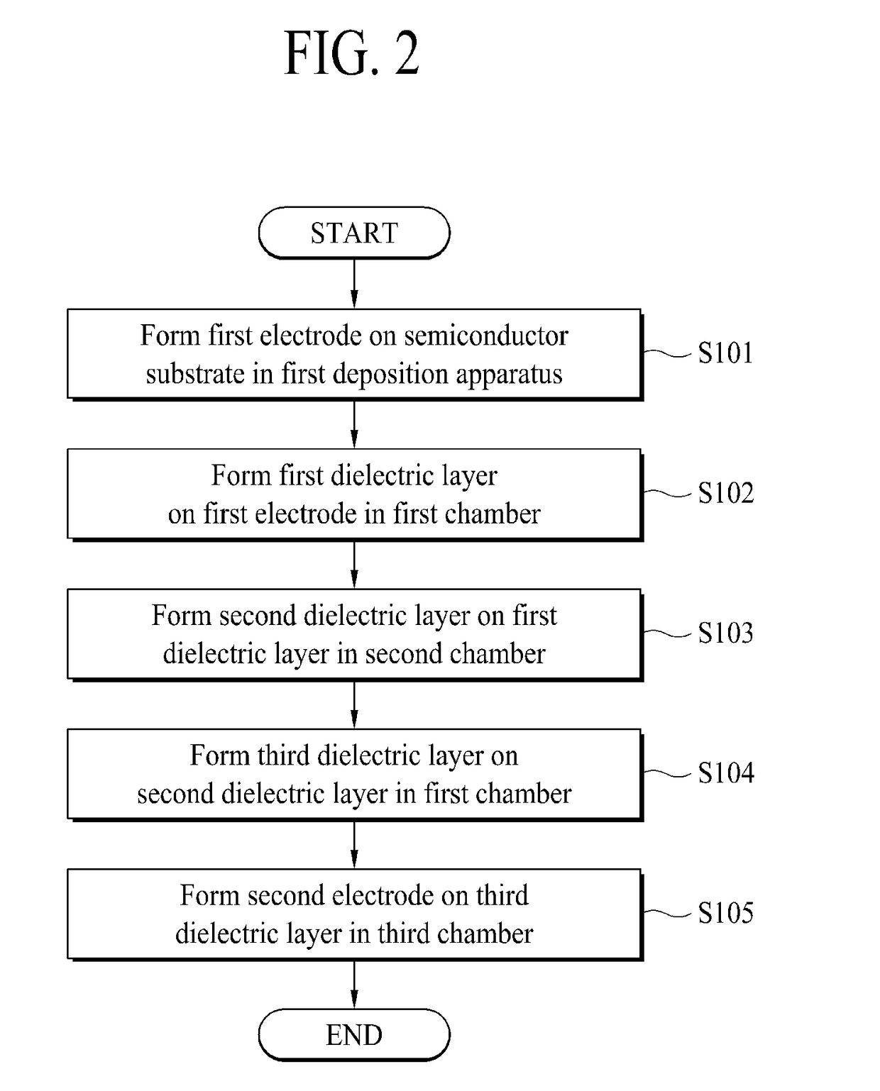
Capacitor deposition apparatus and deposition method of dielectric film using same
a technology of capacitor and dielectric film, which is applied in the direction of electrical equipment, capacitors, basic electric elements, etc., can solve the problems of reducing the quality oxidation or deterioration of the dielectric layer, and difficulty in enlarge the electrode area, so as to prevent the reduction of the capacity of the capacitor, the number of times the semiconductor substrate is loaded and unloaded is reduced, and the capacitor is not easy to enlarge the area
- Summary
- Abstract
- Description
- Claims
- Application Information
AI Technical Summary
Benefits of technology
Problems solved by technology
Method used
Image

Examples
Embodiment Construction
[0045]Reference will now be made in detail to the exemplary embodiments of the present invention, examples of which are illustrated in the accompanying drawings. Wherever possible, the same reference numbers will be used throughout the drawings to refer to the same or like parts.
[0046]Advantages and features of the present invention, and implementation methods thereof will be clarified through following embodiments described with reference to the accompanying drawings. The present invention may, however, be embodied in different forms and should not be construed as limited to the embodiments set forth herein. Rather, these embodiments are provided so that this disclosure will be thorough and complete, and will fully convey the scope of the present invention to those skilled in the art. Further, the present invention is only defined by scopes of claims.
[0047]A shape, a size, a ratio, an angle, and a number disclosed in the drawings for describing embodiments of the present invention ...
PUM
| Property | Measurement | Unit |
|---|---|---|
| dielectric constant | aaaaa | aaaaa |
| dielectric | aaaaa | aaaaa |
| plasma power | aaaaa | aaaaa |
Abstract
Description
Claims
Application Information