CMOS pixel, image sensor, and camera and method for reading out a CMOS pixel

Active Publication Date: 2019-09-26
ROBERT BOSCH GMBH
View PDF10 Cites 4 Cited by
  • Summary
  • Abstract
  • Description
  • Claims
  • Application Information

AI Technical Summary

Benefits of technology

[0047]If the at least one second photodiode is read out using the dual conversion gain readout circuit, which is designed for the at least one first photodiode, this results in a particularly strong amplification factor. Particularly faint objects may thus also be detected via the pixel.
[0048]By adding the photodiode capacitance of the at least one first photodiode, the readout circuit is detuned in such a way that the dual conversion gain readout circuit, which is desi

Problems solved by technology

The challenge in pixel design is to design a circuit which manages with pref

Method used


Image

  • CMOS pixel, image sensor, and camera and method for reading out a CMOS pixel
  • CMOS pixel, image sensor, and camera and method for reading out a CMOS pixel
  • CMOS pixel, image sensor, and camera and method for reading out a CMOS pixel

Examples


Embodiment Construction

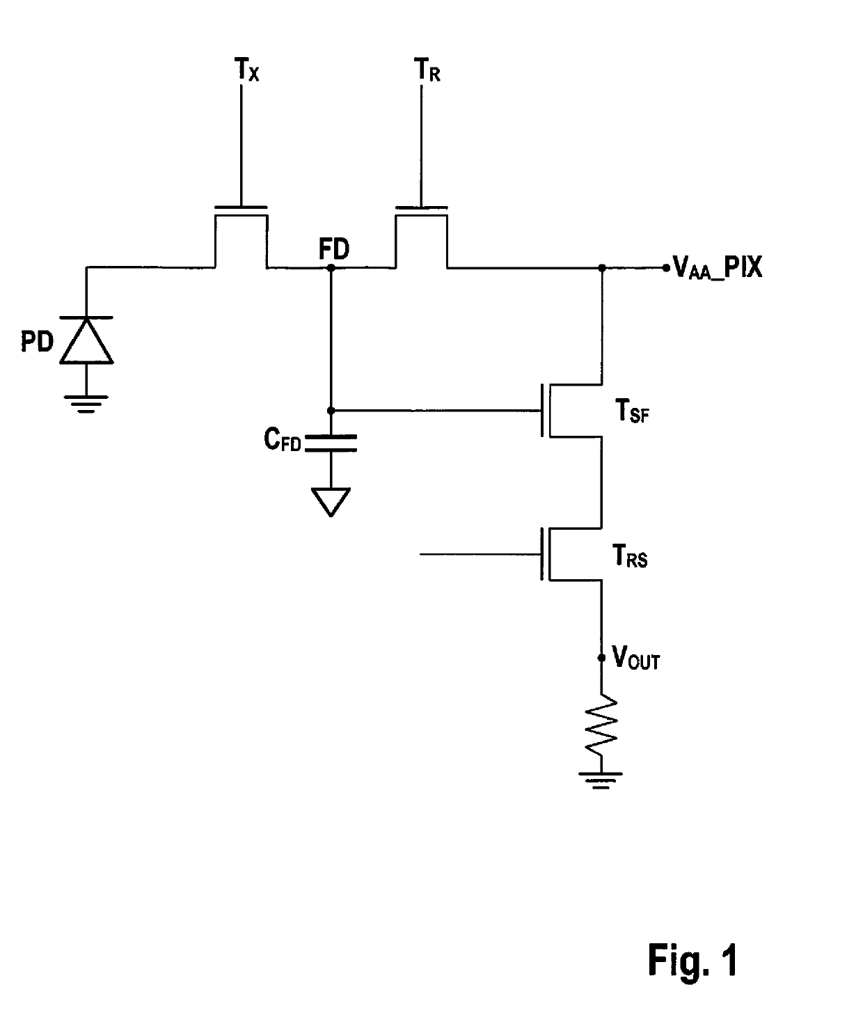
[0053]FIG. 1 shows a CMOS pixel including four transistors according to the related art. The CMOS pixel includes a photodiode PD and a diffusion region FD including an associated capacitance CFD. A transistor is situated as a transfer gate Tx between diffusion region FD and photodiode PD. The charge of photodiode PD is transferred for the readout to diffusion region FD via transfer gate Tx. A transistor is situated as a reset transistor TR between diffusion region FD and voltage supply VAA_PIX of the pixel in order to reset the pixel. Two transistors are situated between voltage supply VAA_PIX and ground as source follower transistor TSF for amplification and as row select transistor TRS for selecting the pixel row to be read out, for example, in rolling shutter operation of a CMOS image sensor made up of CMOS pixels.

[0054]The electromagnetic radiation detected via the pixel, typically light from the ultraviolet to the infrared range, may be read out as a variable represented by a v...


PUM


Abstract

CMOS pixel having a dual conversion gain readout circuit, including at least one first photodiode (PD1), a diffusion region (FD) having a first capacitance (CFD) for accommodating a charge of the at least one first photodiode (PD1), the dual conversion gain readout circuit being designed to read out the charge of the diffusion region (FD) with the aid of a first amplification factor and with the aid of a second amplification factor, the CMOS pixel including at least one second photodiode (PD2), the diffusion region (FD) furthermore being designed to accommodate a charge of the at least one second photodiode (PD2), and the dual conversion gain readout circuit being designed to read out the charge of the diffusion region (FD) with the aid of at least one third amplification factor and at least one fourth amplification factor.

Description

FIELD OF THE INVENTION[0001]The present invention relates to a CMOS pixel, an image sensor, and a camera and a method for reading out a CMOS pixel.BACKGROUND INFORMATION[0002]CMOS image sensors are produced using different pixel designs. Designs having four to six transistors per pixel and one or two photodiodes are typical.[0003]Designs having four transistors and a pinned photodiode are known. Pinned in this context means that the photodiode is manufactured by the silicon process in such a way that the photodiode does not have a connection to a metal.[0004]Furthermore, designs having five transistors, a pinned photodiode, and a dual conversion gain readout circuit are known. A dual conversion gain readout circuit is to be understood in the present case as a circuit which is designed to read out the charge of the photodiode with the aid of at least two different amplification factors, to ascertain the electromagnetic radiation detected by the photodiode, typically in the wavelength...

Claims


Application Information

Patent Timeline
IPC IPC(8): H01L27/146G02B5/02H04N5/378H04N5/355
CPCH01L27/1461H04N5/378G02B5/0205H04N5/3559H04N25/585H04N25/59H04N25/778H04N25/771H04N25/75
Inventor FRITZ, STEFFEN
Owner ROBERT BOSCH GMBH
Why Eureka
Try Eureka