

Low-cost semiconductor package using conductive metal structure
- Summary
- Abstract
- Description
- Claims
- Application Information
AI Technical Summary
Benefits of technology
Problems solved by technology
Method used
Image

Examples
Embodiment Construction
[0020]Hereinafter, the present invention will be described in detail by explaining exemplary embodiments of the invention with reference to the attached drawings. In the description of the present invention, certain detailed explanations of related art are omitted when it is deemed that they may unnecessarily obscure the essence of the invention.
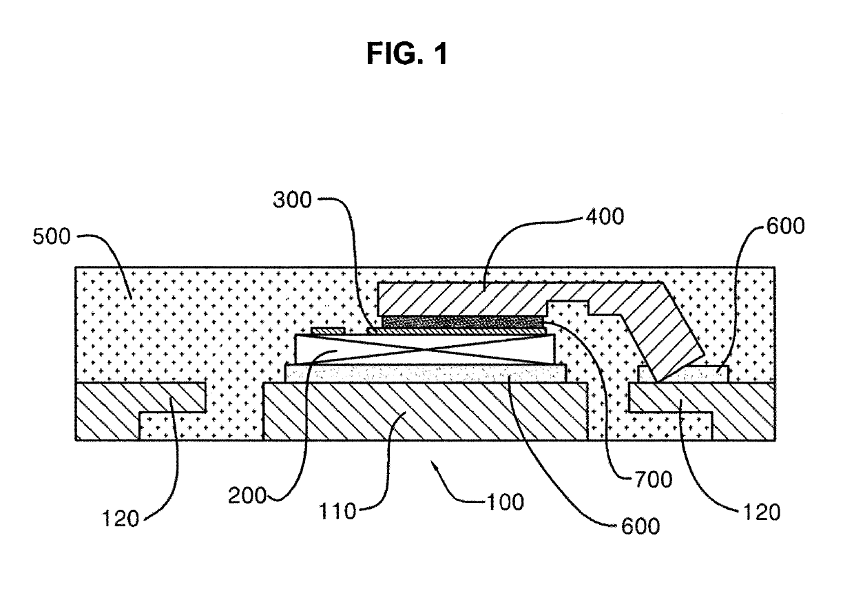
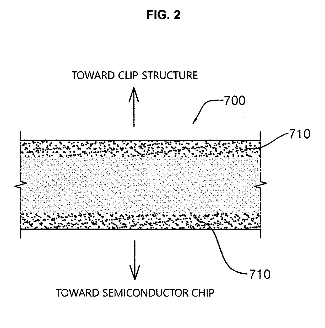
[0021]As shown in FIG. 1, a low-cost semiconductor package using a conductive metal structure according to the present invention may include a lead frame 100 including a pad 110 and a lead 120, a semiconductor chip 200 attached onto the pad 110 of the lead frame 100, an Aluminum (Al) pad 300 formed on the semiconductor chip 200, a clip structure 400 having one side adhered to the Al pad 300 and the other side adhered to the lead 120 of the lead frame 100, and a sealing member 500 formed to surround the semiconductor chip 200 and the clip structure 400 via molding.
[0022]The semiconductor chip 200 may be adhered directly to a junction of the l...
PUM
 Abstract
Description
Claims
Application Information