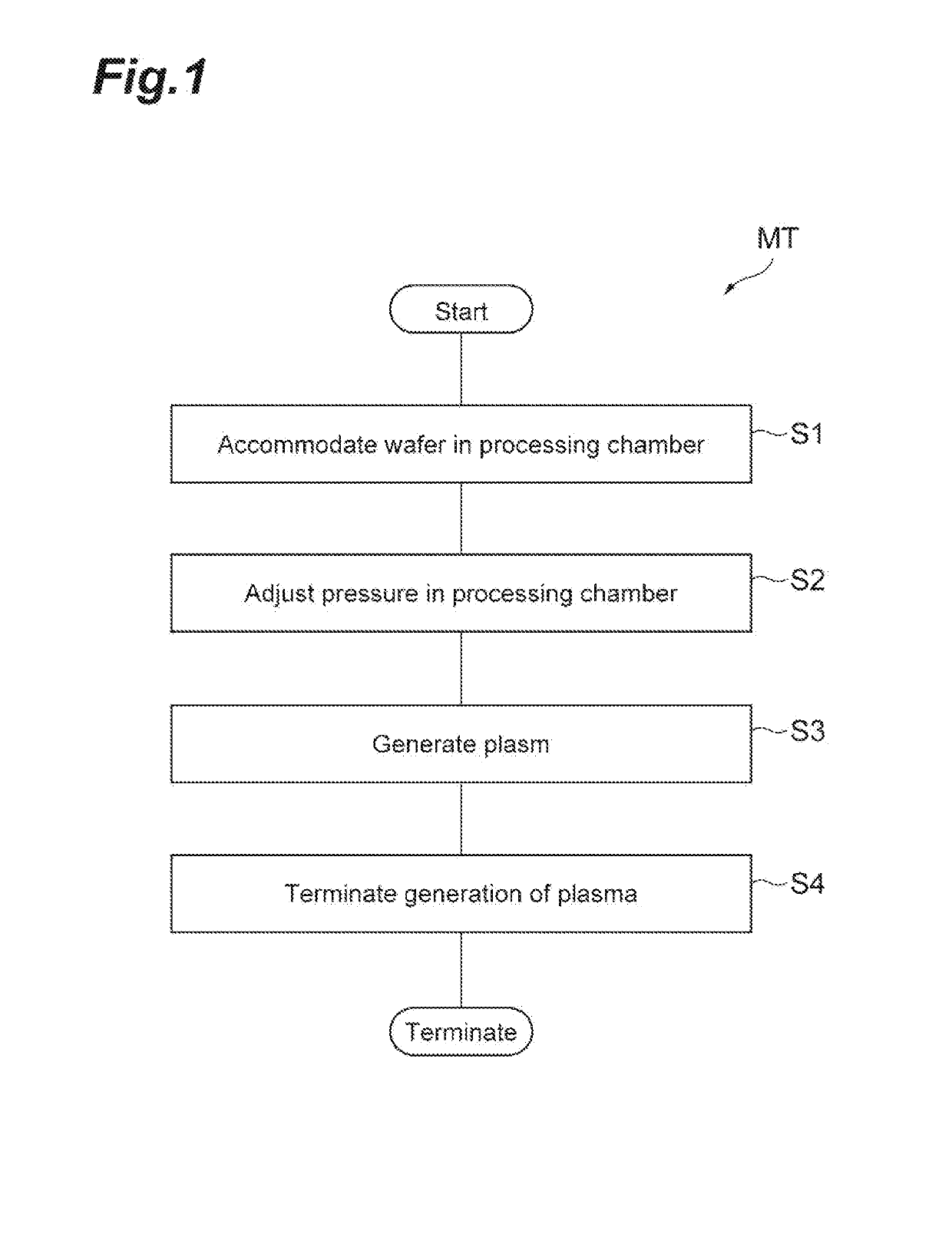
Method for processing workpiece
a technology for workpieces and workpieces, applied in the direction of coatings, chemical vapor deposition coatings, electric discharge tubes, etc., can solve problems such as difficulties accompanied by technological development, and achieve the effect of suppressing process complication
- Summary
- Abstract
- Description
- Claims
- Application Information
AI Technical Summary
Benefits of technology
Problems solved by technology
Method used
Image

Examples
example 1
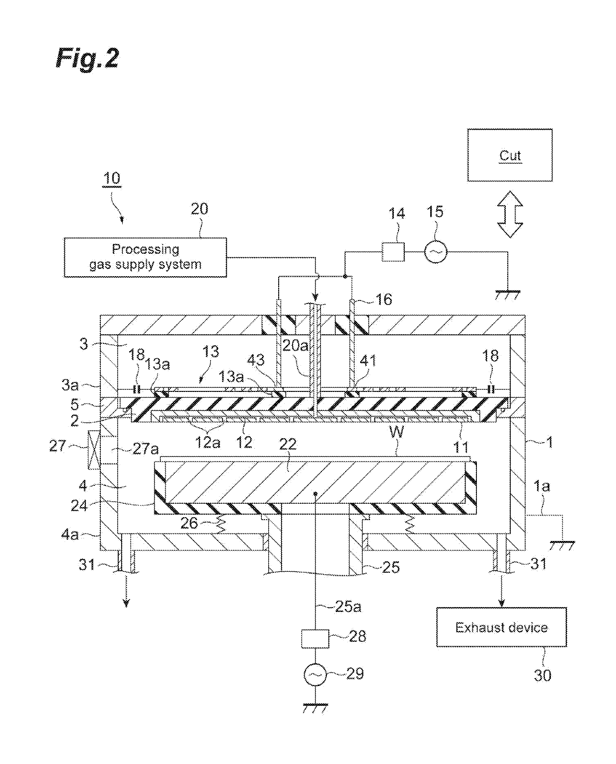
[0055]Steps S2 and S3 can be implemented under the following condition, for example. In addition, the following condition is a condition in a case where the precoat film PC is not formed on the surface on the inner side of the processing chamber 4.
[0056]Value [Pa] of pressure in processing chamber 4: 0.1 to 10 [Pa]
[0057]Value [MHz] of frequency of high-frequency power source 15 and value [watt] of high-frequency power: 13.56 [MHz], 100 to 5000 [watt]
[0058]Value [MHz] of frequency of high-frequency power source 29 and value [watt] of bias power: 0.4 to 6 [MHz], 0 to 500 [watt]
[0059]Processing gas: O2 gas (first gas), SiF4 gas (second gas)
example 2
[0060]There is a case where the precoat film PC that contains silicon and halogen is formed on the surface on the inner side of the processing chamber 4 used in step S1. The film thickness of the precoat film PC is approximately 100 [nm] or less. In addition, the precoat film PC is foamed almost entirely on the inside of the processing chamber 4.
example 3
[0061]Steps S2 to S4 were executed by using the following process condition A using each of Si, th-Ox (thermal oxide film), SiN, SiCOH, and Cu as the materials of the underlayer, and the results illustrated in FIGS. 6 and 7 were obtained. FIG. 6 is a view illustrating the result of examples obtained for each material of the underlayer. The horizontal axis of FIG. 6 represents the execution time [sec] of step S3, and the vertical axis of FIG. 6 represents the thickness (film thickness) [nm] of the laminated film. FIG. 7 is a view illustrating the result obtained under various process conditions. The horizontal axis on the upper side of FIG. 7 represents the temperature [° C.] (T[° C.]) of the wafer W (underlayer) at the time of execution of step S3, the horizontal axis on the lower side of FIG. 7 represents the value (1000 / T) obtained by multiplying the inverse number of T[° C.] by 1000, and the vertical axis in FIG. 7 represents the deposition rate [nm / sec] of the film.
Process Condi...
PUM
| Property | Measurement | Unit |
|---|---|---|
| temperature | aaaaa | aaaaa |
| frequency | aaaaa | aaaaa |
| frequency | aaaaa | aaaaa |
Abstract
Description
Claims
Application Information
 - R&D
- Intellectual Property
- Life Sciences
- Materials
- Tech Scout
- Unparalleled Data Quality
- Higher Quality Content
- 60% Fewer Hallucinations
Browse by: Latest US Patents, China's latest patents, Technical Efficacy Thesaurus, Application Domain, Technology Topic, Popular Technical Reports.
© 2025 PatSnap. All rights reserved.Legal|Privacy policy|Modern Slavery Act Transparency Statement|Sitemap|About US| Contact US: help@patsnap.com