Manufacturing method of micro light-emitting diode display panel and micro light-emitting diode display panel

a manufacturing method and technology of micro light-emitting diodes, applied in the field of display, can solve the problems that the upper electrode of the micro led and the upper electrode of the pixel electrode cannot be electrically connected, and achieve the effects of avoiding poor connection, and improving the assembling result of the micro led

Active Publication Date: 2019-10-31
TCL CHINA STAR OPTOELECTRONICS TECH CO LTD
View PDF5 Cites 10 Cited by
  • Summary
  • Abstract
  • Description
  • Claims
  • Application Information

AI Technical Summary

Benefits of technology

[0006]The object of the present invention is to provide a manufacturing method of micro LED display panel, able to improve the pair-assembling effect of the micro LED display panel and avoid poor connection between the upper pixel electrode and the upper electrode of the micro LED.
[0007]Another object of the present invention is to provide a micro LED display panel, able to improve the pair-assembling effect of the micro LED display panel and avoid poor connection between the upper pixel electrode and the upper electrode of the micro LED.
[0027]The present invention provides the following advantages: the present invention provides a manufacturing method of micro LED display panel, which forms an elastic conductive layer on upper pixel electrode on package substrate, and realizes electrical connection between the upper pixel electrode and upper electrode of the micro LED when pair-assembling the package substrate and driving substrate. By utilizing the elasticity of the elastic conductive layer to fill in the height difference between the micro LEDs to avoid poor connection between the upper pixel electrode and the upper electrode of the micro LED, the invention improves the assembling result of the micro LED and the process yield. The present invention also provides a micro LED display panel, which can improve the assembling result of the micro LED and avoid poor connection between the upper pixel electrode and the upper electrode of the micro LED.

Problems solved by technology

When pair-assembling the package substrate and the drive substrate, because the top of the micro LED is uneven, that is, the height of each micro LED is not entirely the same, a part of upper pixel electrodes may not correctly attach to the upper electrodes of the micro LED, which results in the problem that the upper pixel electrode and the upper electrode of the micro LED cannot be electrically connected.

Method used


Image

  • Manufacturing method of micro light-emitting diode display panel and micro light-emitting diode display panel
  • Manufacturing method of micro light-emitting diode display panel and micro light-emitting diode display panel
  • Manufacturing method of micro light-emitting diode display panel and micro light-emitting diode display panel

Examples


first embodiment

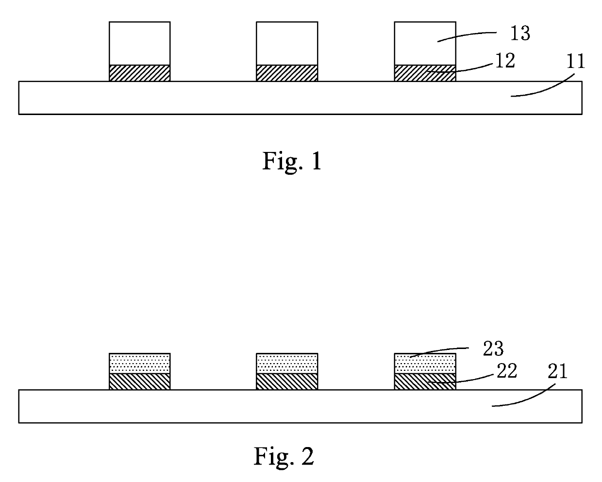
[0039]Specifically, in the present invention, the first solution comprises a first solvent and a plurality of elastic conductive balls dispersed in the first solvent, and the first solvent is a curable solvent. Preferably, the first solvent is a resin solvent or other curable solvent. The elastic conductive ball is a nanometer or micron-sized silicon dioxide ball having outer surface coated with a conductive material, or the elastic conductive ball is a gold (Au) ball. The conductive material covering the silicon dioxide may be carbon nanotubes.

[0040]Moreover, in the first embodiment, in step S3, a curing process is performed while the package substrate 21 and the driving substrate 11 are pair-assembled and pressed, so that the first solvent in the elastic conductive layer 23 is cured. The curing process may be selected from heat curing or ultraviolet light curing depending on the properties of the first solvent.

[0041]Moreover, in the first embodiment, before the first solvent is cu...

second embodiment

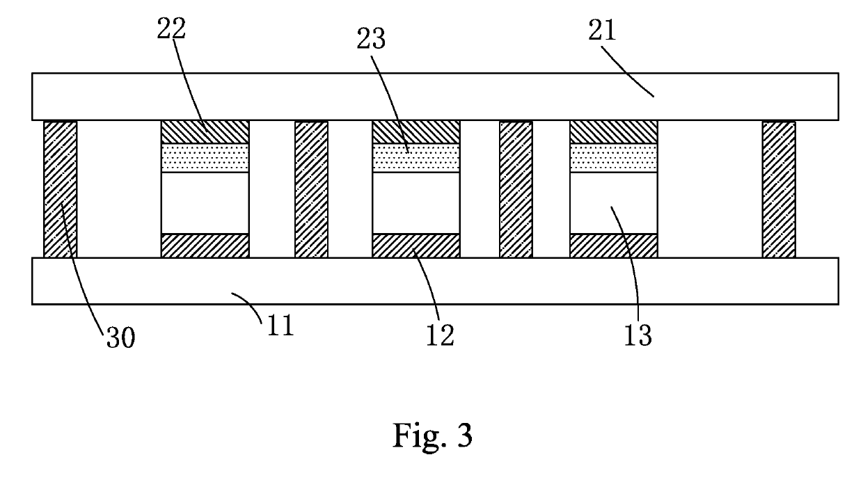
[0043]Specifically, in the present invention, in step S2, the elastic conductive layer 23 is formed by coating an elastic conductive adhesive on each upper pixel electrode 22.

[0044]It should be noted that the thickness of the elastic conductive layer 23 in a natural state after the pair-assembling (before pressing) should be greater than the distance from the upper electrode of the lowest-level Micro LED 13 to the corresponding upper pixel electrode 22 so that after the elastic conductive layers 23 is pressed, the entire elastic conductive layers 23 can contact the upper electrode of the corresponding Micro LED 13. As such, the upper pixel electrode 22 and the upper electrode of the Micro LED 13 maintain good Ohmic contact.

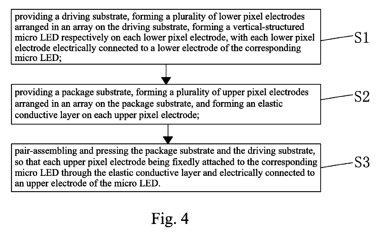
[0045]Specifically, to improve the pressure-endurance capability of the drive substrate 11 and the package substrate 21, the present invention further comprises the step of forming a support 30 on the driving substrate 11 or the package substrate 21 before the pac...


PUM


Abstract

The invention provides a manufacturing method of micro LED display panel and micro LED display panel. In the manufacturing method, an elastic conductive layer is formed on the upper pixel electrode on the package substrate. When the package substrate and the driving substrate are assembled, the upper pixel electrode and the upper electrode of the micro LED are electrically connected through the elastic conductive layer, and the elasticity of the elastic conductive layer is utilized to fill the height difference between the individual micro LEDs, avoid poor connection between the upper pixel electrode and the upper electrode of the micro LED, and improve the assembling effect of the micro LED display panel and the process yield of the micro LED display panel.

Description

BACKGROUND OF THE INVENTION1. Field of the Invention[0001]The present invention relates to the field of display, and in particular to a manufacturing method of micro light-emitting diode (micro LED) display panel and micro LED display panel.2. The Related Arts[0002]With the rapid development of wearable display devices, micro-LED (uLED) technology has emerged. The micro LED technology, i.e., the LED micro-reduction and matrixing technology, refers to a high-density, micro-sized LED array that is integrated on a single chip. The power consumption of the micro LED is much lower than that of a liquid crystal display (LCD), is self-luminous like an organic light-emitting diode (OLED), and can reduce the distance between the pixels from the millimeter level to the micrometer level. Also, the color saturation is close to OLED, so many manufacturers regard micro LED as the display technology of the next generation.[0003]The known micro LED array is fabricated by a micro transfer printing m...

Claims


Application Information

Patent Timeline
Patent Type & Authority Applications(United States)
IPC IPC(8): H01L25/075H01L33/62H01L33/36H01L33/44
CPCH01L33/36H01L25/0753H01L2933/0016H01L2933/0033H01L2933/0066H01L33/62H01L33/44H01L25/167H01L33/0095
Inventor CHEN, LIXUAN
Owner TCL CHINA STAR OPTOELECTRONICS TECH CO LTD
Why Eureka
Try Eureka