Substrate for front side type imager and method of manufacturing such a substrate
- Summary
- Abstract
- Description
- Claims
- Application Information
AI Technical Summary
Benefits of technology
Problems solved by technology
Method used
Image

Examples
first embodiment
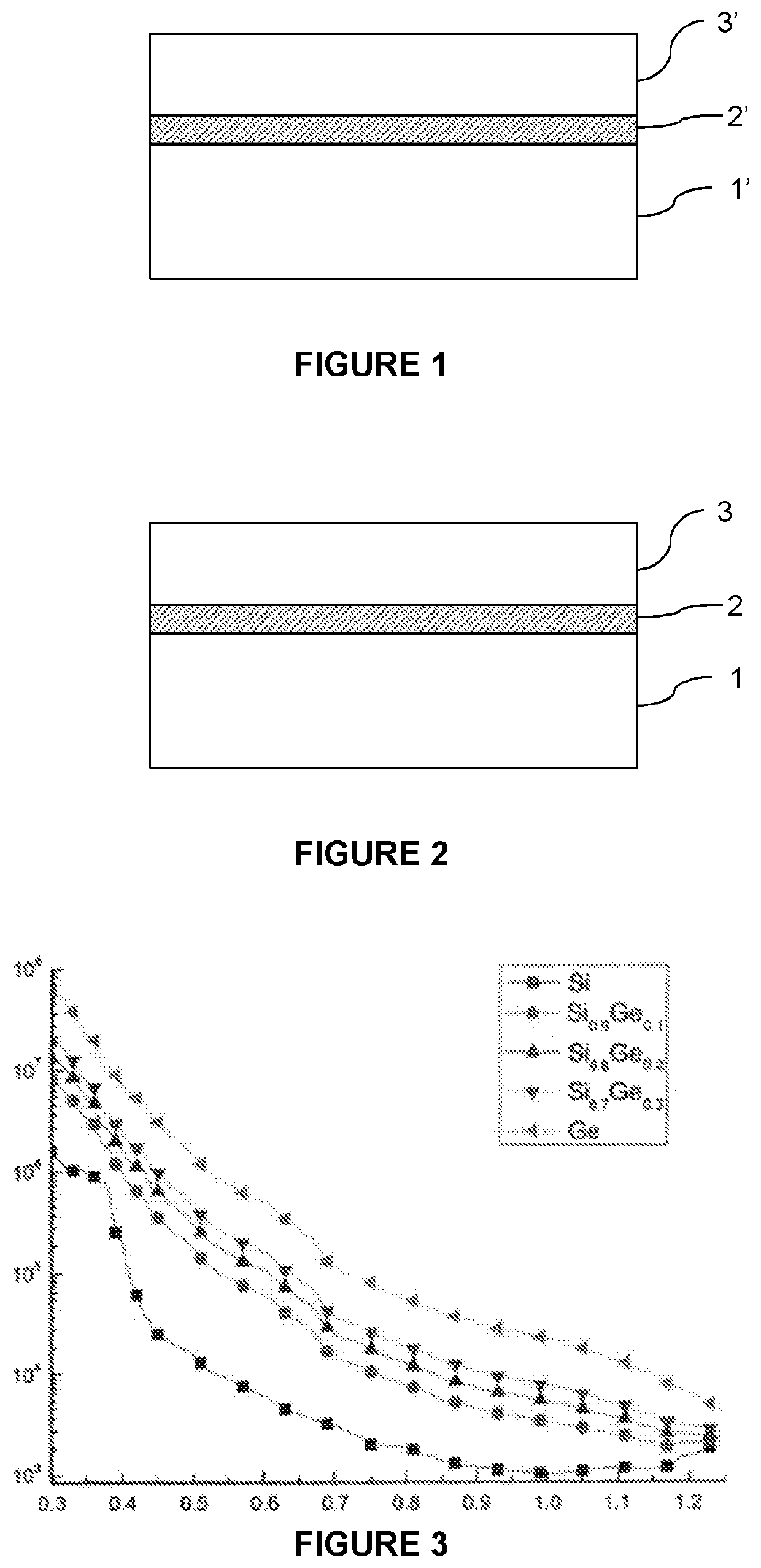
[0080] illustrated in FIGS. 6A to 6F, the starting point is a donor substrate 30 comprising a superficial SiGe layer 31.
[0081]The SiGe layer 31 is typically formed by epitaxy on a base substrate 32, generally made of silicon. The SiGe layer 31 is sufficiently thin to be stressed.
[0082]In a first version of this embodiment, an embrittlement zone 33 is formed in the SiGe layer, as illustrated in FIG. 6B.
[0083]In a particularly advantageous manner, the embrittlement zone 33 is formed by implantation of atomic species (typically, hydrogen and / or helium) through the free surface of the SiGe layer 31. The embrittlement zone 33 thereby delimits a SiGe layer 34 at the surface of the donor substrate.
[0084]With reference to FIG. 6C, a receiver substrate is moreover provided comprising a support substrate 1 and an electrically insulating layer 2.
[0085]With reference to FIG. 6D, the donor substrate is bonded onto the receiver substrate, the SiGe layer 31 and the electrically insulating layer 2 ...
second embodiment
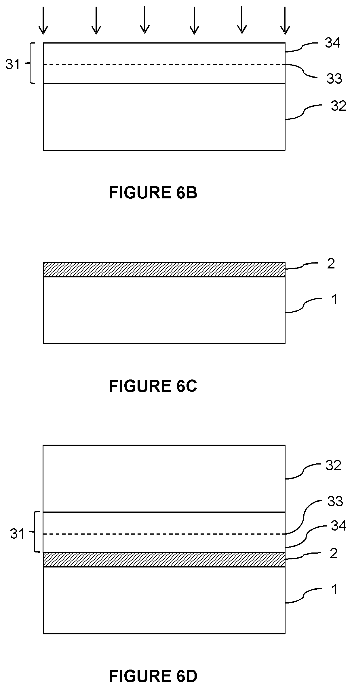
[0099] illustrated in FIGS. 8A to 8D, the well-known Smart Cut™ method is used to form a SOI substrate comprising the support substrate, the electrically insulating layer, and a silicon seed layer intended for the epitaxial growth of the SiGe layer.
[0100]To this end, a donor silicon substrate 40 covered by the electrically insulating layer 2 as shown in FIG. 8A is provided, then an embrittlement zone 41 delimiting a silicon layer 42 to transfer is formed by implantation of atomic species, as shown in FIG. 8B.
[0101]A receiver substrate is moreover provided, which is typically the support substrate 1 of the final substrate.
[0102]With reference to FIG. 8C, the donor substrate 40 is bonded on the receiver substrate 1, the electrically insulating layer 2 being present at the bonding interface.
[0103]Next, the donor substrate is detached along the embrittlement zone. The detachment may be initiated by any technique known to those skilled in the art, such as by application of mechanical, ch...
PUM
 Abstract
Description
Claims
Application Information
 - Generate Ideas
- Intellectual Property
- Life Sciences
- Materials
- Tech Scout
- Unparalleled Data Quality
- Higher Quality Content
- 60% Fewer Hallucinations
Browse by: Latest US Patents, China's latest patents, Technical Efficacy Thesaurus, Application Domain, Technology Topic, Popular Technical Reports.
© 2025 PatSnap. All rights reserved.Legal|Privacy policy|Modern Slavery Act Transparency Statement|Sitemap|About US| Contact US: help@patsnap.com