Methods for repairing substrate lattice and selective epitaxy processing

a technology of epitaxy and substrate, applied in the direction of basic electric elements, semiconductor/solid-state device manufacturing, electrical equipment, etc., can solve the problems of corroding the channel hole, affecting the epitaxial growth rate and thickness of the epitaxial layer in the seed window area, and the substrate surface is not uniform, so as to achieve the effect of low energy and higher energy

Active Publication Date: 2019-11-28
YANGTZE MEMORY TECH CO LTD
View PDF0 Cites 145 Cited by
  • Summary
  • Abstract
  • Description
  • Claims
  • Application Information

AI Technical Summary

Benefits of technology

[0007]In some embodiments, forming the amorphous layer includes ion implantation. The total dosage of the implantation is greater than 5×10¹⁵ ion/cm3. The implant temperature is −100° C. to 23° C. The implant energy is 25 keV to 250 keV. The implanted material includes one or more of III element, IV element, V element, and inert element. The implanted material includes one or more of silicon, carbon,

Problems solved by technology

With the scaling down of device dimensions, such as for three-dimensional (3D) NAND flash memory devices, reduced seed window area dimensions and SEG pre-cleaning processes can cause non-uniformity in the substrate surface.
In particular, SEG pre-cleaning processes can greatly affect the epitaxial growth rate and thickness of an epitaxial layer in the seed window area, as well as corrode the channel hole.
Significant substrate lattice damage can occur when a channel hole is formed in a patterne

Method used


Image

  • Methods for repairing substrate lattice and selective epitaxy processing
  • Methods for repairing substrate lattice and selective epitaxy processing
  • Methods for repairing substrate lattice and selective epitaxy processing

Examples


Embodiment Construction

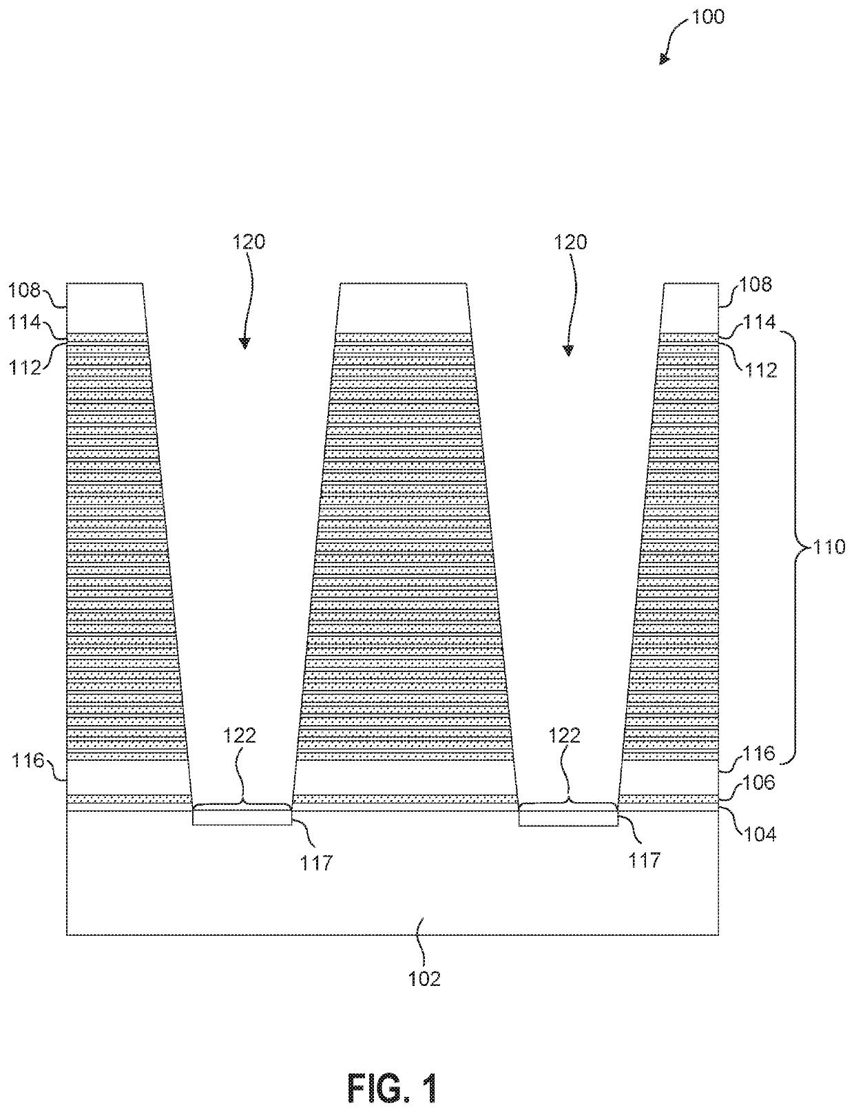
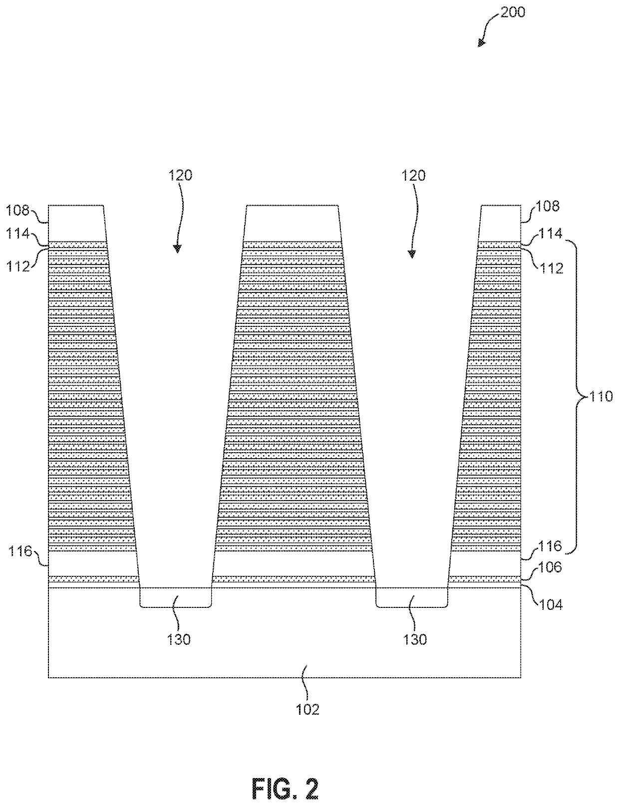
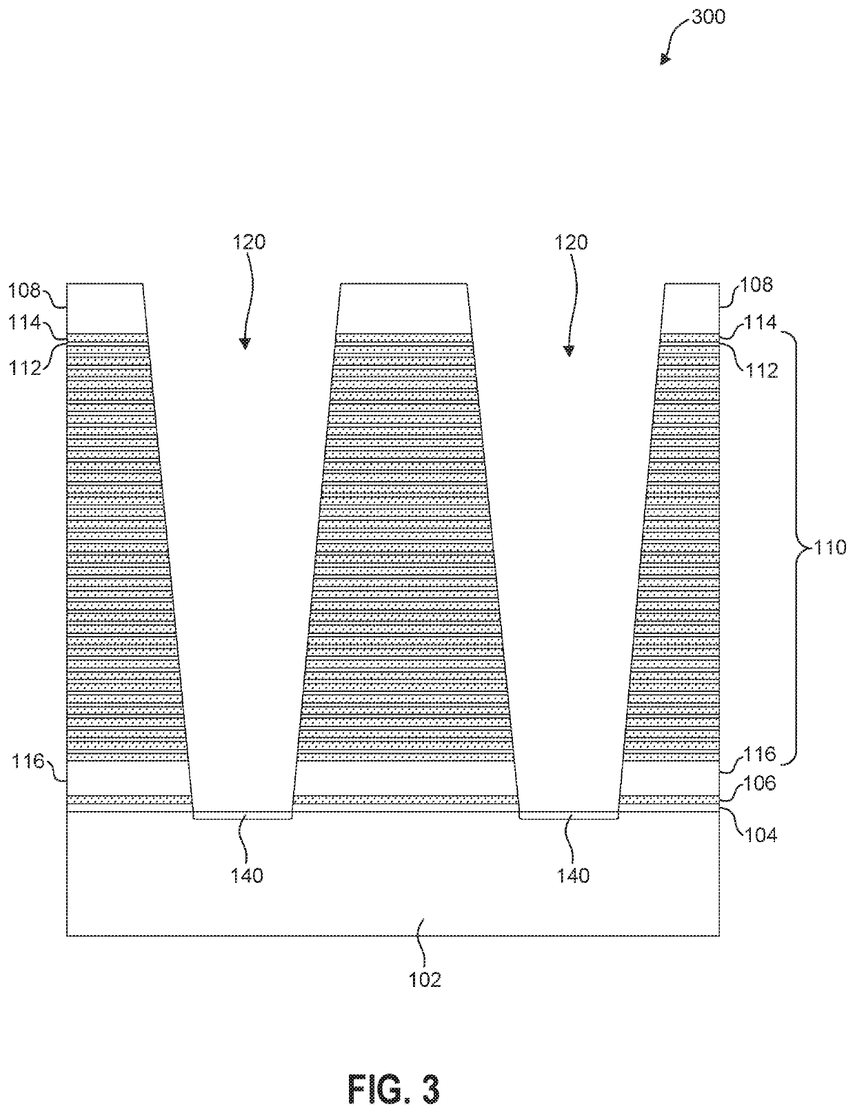
[0017]Although specific configurations and arrangements are discussed, it should be understood that this is done for illustrative purposes only. A person skilled in the pertinent art will recognize that other configurations and arrangements can be used without departing from the spirit and scope of the present disclosure. It will be apparent to a person skilled in the pertinent art that the present disclosure can also be employed in a variety of other applications.

[0018]It is noted that references in the specification to “one embodiment,”“an embodiment,”“an example embodiment,”“some embodiments,” etc., indicate that the embodiment described may include a particular feature, structure, or characteristic, but every embodiment may not necessarily include the particular feature, structure, or characteristic. Moreover, such phrases do not necessarily refer to the same embodiment. Further, when a particular feature, structure or characteristic is described in connection with an embodiment...


PUM


Abstract

The present disclosure describes patterned devices and methods for repairing substrate lattice damage in a patterned device. The patterned device includes a substrate, an alternating conductor and dielectric stack atop the substrate, a channel hole extending through the alternating conductor and dielectric stack to the substrate, and an epitaxial grown layer at a bottom of the channel hole and a top surface of the substrate. A part of the substrate in contact with the epitaxial grown layer has a dopant or doping concentration different from an adjacent part of the substrate. The method includes forming a channel hole in an insulating layer atop a substrate, forming an amorphous layer in a top side of the substrate below the channel hole, heating to crystallize the amorphous layer, and growing an epitaxial layer on the crystallized layer in the channel hole.

Description

BACKGROUND[0001]Epitaxy is the growth of a crystalline layer, typically from a seed layer. Selective epitaxial growth (SEG) is one type of epitaxy adapted for growth of a single crystalline layer on only a selected portion(s) of a substrate called seed window areas in a channel hole. The surface of the substrate can be selectively exposed by removing an intervening protective layer to form a seed window area. With the scaling down of device dimensions, such as for three-dimensional (3D) NAND flash memory devices, reduced seed window area dimensions and SEG pre-cleaning processes can cause non-uniformity in the substrate surface. In particular, SEG pre-cleaning processes can greatly affect the epitaxial growth rate and thickness of an epitaxial layer in the seed window area, as well as corrode the channel hole.[0002]Significant substrate lattice damage can occur when a channel hole is formed in a patterned device. Normally hydrogen chloride (HCl) gas will be used to remove a damaged ...

Claims


Application Information

Patent Timeline
IPC IPC(8): H01L21/02
CPCH01L21/265H01L21/324H10B41/20H10B41/35H01L21/02645H01L21/02642H10B41/27H10B43/27H01L21/0245H01L21/02513H01L21/02658H01L21/26513H01L21/26533H01L21/31116H10B69/00
Inventor WANG, XIAO JUNZHOU, WEIXU, LIN KANGLI, GUAN NAN
Owner YANGTZE MEMORY TECH CO LTD
Why Eureka
Try Eureka