Nonvolatile memory apparatus, and read and write method of the nonvolatile memory apparatus

a non-volatile memory and flash memory technology, applied in the field of semiconductor technology, can solve the problems of flash memory apparatus, slow data storage speed, loss of stored data, etc., and achieve the effect of increasing an amount of curren

Active Publication Date: 2019-12-19
SK HYNIX INC
View PDF14 Cites 7 Cited by
  • Summary
  • Abstract
  • Description
  • Claims
  • Application Information

AI Technical Summary

Benefits of technology

[0005]In an embodiment of the present disclosure, a non-volatile memory apparatus may include a memory cell, a bit line control circuit, a snap-back detection circuit, and a word line control circuit. The memory cell may be coupled between a global bit line and a global word line. The bit line control circuit may be configured to apply a bit line read bias voltage to the global bit line based on a read signal. The snap-back detection circuit may be coupled to the global word line, and may be configured to generate a data output signal and a current enable signal by detecting a snap-back of the memory cell. The word line control circuit may be configured to apply a word line read bias voltage to the global word line based on the read signal, and may increase an amount of a current flowing through the memory cell based on the current enable signal.
[0006]In an embodiment of the present disclosure, a non-volatile memory apparatus may include a memory cell, a bit line control circuit, a snap-back detection circuit, and a word line control circuit. The memory cell may be coupled between a global bit line and a global word line. The bit line control circuit may be configured to apply a bit line write bias voltage to the global bit line based on a write signal, and may variably change a voltage level of the global bit line based on the write signal and a current enable signal. The snap-back detection circuit may be coupled to the global word line, and may be configured to generate the current enable signal by detecting a snap-back of the memory cell. The word line control circuit may be configured to apply a word line write bias voltage to the global word line based on the write signal, and may increase an amount of a current flowing through the memory cell based on the current enable signal.
[0007]In an embodiment of the present disclosure, a read method of a non-volatile memory apparatus may include applying a read voltage, which is for causing a snap-back in a memory cell of a low resistance state, across a memory cell. The read method may include selectively increasing an amount of a current flowing the memory cell according to whether a snap-back of the memory cell occurs.
[0008]In an embodiment of the present disclosure, a write method of a non-volatile memory apparatus may include applying a write voltage, which is for causing a snap-back in a memory cell of a low resistance state or a memory cell of a high resistance state, across a memory cell coupled between a global bit line and a global word line; and may change an amount of a current flowing the memory cell according to a write signal and whether a snap-back of the memory cell occurs.

Problems solved by technology

However, the DRAM has a volatile characteristic whereby it loses stored data when powered off since it has a memory cell comprising a capacitor.
However, the flash memory apparatus has disadvantages because it stores and outputs data at a slow speed and is not random accessible, when compared with the DRAM.

Method used


Image

  • Nonvolatile memory apparatus, and read and write method of the nonvolatile memory apparatus
  • Nonvolatile memory apparatus, and read and write method of the nonvolatile memory apparatus
  • Nonvolatile memory apparatus, and read and write method of the nonvolatile memory apparatus

Examples


Embodiment Construction

[0019]Hereinafter, a semiconductor apparatus according to the present disclosure will be described below with reference to the accompanying drawings through various embodiments.

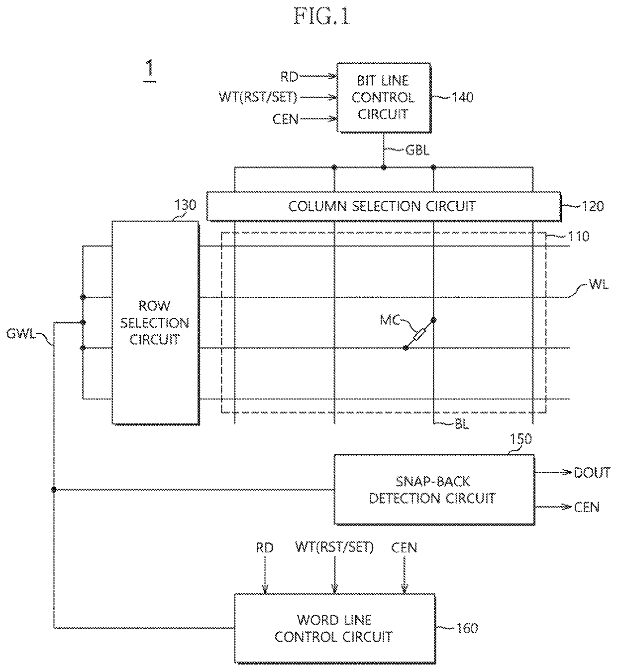
[0020]FIG. 1 is a diagram illustrating a configuration of a non-volatile memory apparatus 1 in accordance with an embodiment of the present disclosure. Referring to FIG. 1, the non-volatile memory apparatus 1 may include a memory array 110. A plurality of bit lines BL may be disposed in a column direction of the memory array 110 and a plurality of word lines WL may be disposed in a row direction of the memory array 110. A plurality of memory cells MC may be coupled to cross points formed by the plurality of bit lines BL and the plurality of word lines WL. Each of the plurality of memory cells MC may be coupled between a corresponding bit line BL and a corresponding word line WL among the plurality of bit lines BL and the plurality of word lines WL. Each of the plurality of memory cells MC may be configured by...


PUM


Abstract

A non-volatile memory apparatus includes a memory cell coupled between a global bit line and a global word line. A bit line control circuit configured to apply a bit line read bias voltage to the global bit line based on a read signal. A snap-back detection circuit coupled to the global word line, and configured to generate a data output signal and a current enable signal by detecting a snap-back of the memory cell. A word line control circuit configured to apply a word line read bias voltage to the global word line based on the read signal, and may increase an amount of a current flowing through the memory cell based on the current enable signal.

Description

CROSS-REFERENCES TO RELATED APPLICATION[0001]The present application claims priority under 35 U.S.C. § 119(a) to Korean application number 10-2018-0069622, filed on Jun. 18, 2018, in the Korean Intellectual Property Office, which is incorporated herein by reference in its entirety.BACKGROUND1. Technical Field[0002]Various embodiments of the present disclosure generally relate to a semiconductor technology and, more particularly, to a non-volatile memory apparatus and read and write method of the non-volatile memory apparatus.2. Related Art[0003]An electronic device includes a lot of electronic elements, and a computer system includes lots of semiconductor apparatuses each comprising a semiconductor. The computer system may include a memory apparatus. A dynamic random access memory (DRAM) is widely used as a general memory apparatus because of advantages it provides regarding the storage and outputting of data at fast and steady speeds with random access. However, the DRAM has a vola...

Claims


Application Information

Patent Timeline
Patent Type & Authority Applications(United States)
IPC IPC(8): G11C5/06G11C5/14G11C13/00G05F3/02
CPCG05F3/02G11C5/063G11C2013/0045G11C5/147G11C13/004G11C16/08G11C16/10G11C16/24G11C16/26G11C13/0004G11C13/0028G11C13/0069G11C8/08G11C7/18G11C7/06G11C7/12G11C2207/063G11C13/0033
Inventor KANG, SEOK JOONPARK, JIN SUEM, HO SEOK
Owner SK HYNIX INC
Why Eureka
Try Eureka