Differential Coating of High Aspect Ratio Objects Through Methods of Reduced Flow and Dosing Variations

a technology of high aspect ratio and differential coating, which is applied in the direction of multiplier dynodes, electron multiplier details, multiplication electrode arrangements, etc., can solve the problems of high manufacturing cost, fragile and easily broken, and bulky and relatively complicated, and achieve high aspect ratio

Active Publication Date: 2020-01-02
PHOTONIS SCI INC
View PDF0 Cites 0 Cited by
  • Summary
  • Abstract
  • Description
  • Claims
  • Application Information

AI Technical Summary

Benefits of technology

[0007]In accordance with a first aspect of this invention there is provided a channel electron multiplier that includes a high aspect ratio elongated tube having a length (L) and an internal diameter (D) wherein L>>D. The elongated tube has an input end, an output end, and an interior surface extending along the length of the tube between the input end and the output end. The channel electron multiplier also has first and second sections of conductive layers formed on the interior surface of the tube. The first conductive layer is formed on the interior surface in a first zone of the elongated tube. The first conductive layer has a length I1 that is less than L and the first conductive layer is selected to provide a first electrical resistance, a first electron emission characteristic, or both. The second conductive layer is formed on the interior surface in a second zone of the elongated tube that does not overlap with the first zone. The second conductive layer has a length I2 that is the difference between L and I1. The second conductive layer is selected to provide a second electrical resistance, a second electron emission characteristic, or both. The channel electron multiplier of this invention also includes a first electrode formed on the elongated tube at the input end thereof and a second electrode formed on the elongated tube at the output end thereof. Although the foregoing describes embodiments of the method as applied to detectors fabricated from straight tubes it is to be understood the invention applies to CEMs having any channel shape or form either singly or in combination with other sections.
[0008]In ac...

Problems solved by technology

However, they are bulky and relatively complicated and can be expensive to manufacture.
These plates typically are biased to lower voltages than the other two detector types, are fragile and easily b...

Method used


Image

  • Differential Coating of High Aspect Ratio Objects Through Methods of Reduced Flow and Dosing Variations
  • Differential Coating of High Aspect Ratio Objects Through Methods of Reduced Flow and Dosing Variations
  • Differential Coating of High Aspect Ratio Objects Through Methods of Reduced Flow and Dosing Variations

Examples


second embodiment

[0021]It is also contemplated that the channel electron multiplier according to the present invention can be made with more than two coating zones. Referring to FIG. 2, there is shown a channel electron multiplier according to the invention. The embodiment shown in FIG. 2 has a graduated electrical resistance along the internal surface of the tube. The graduated resistance is provided by forming a plurality of resistive coatings in very small, adjacent zones sequentially along the length of the internal surface. The coating in each zone is selected to provide an incrementally different electrical resistance relative to the coatings in the adjacent zones on either side. Thus, the coating materials can be selected to provide a gradually increasing electrical resistance from the input end to the output end or a gradually decreasing electrical resistance from the input end to the output end.

third embodiment

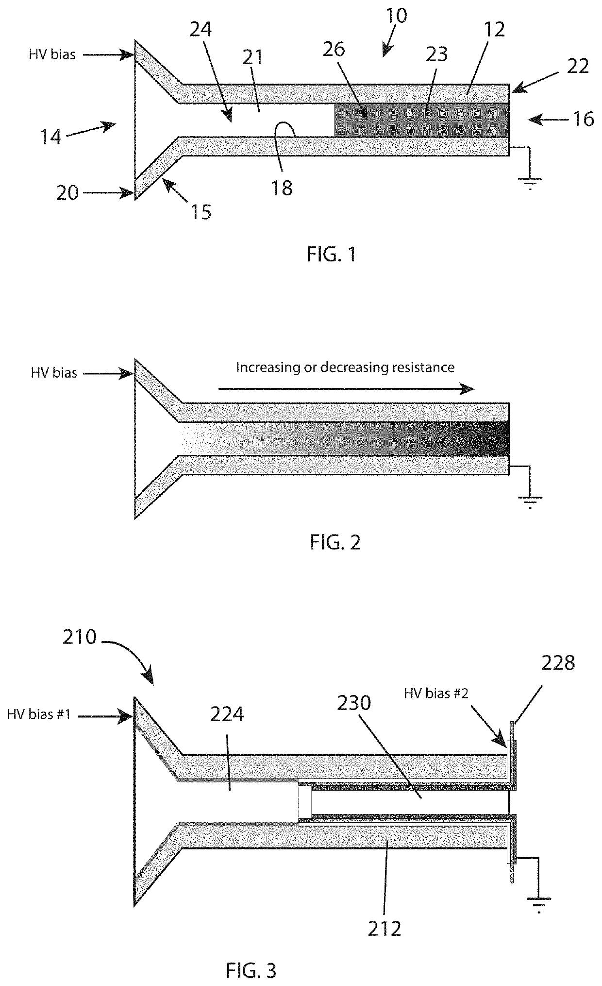
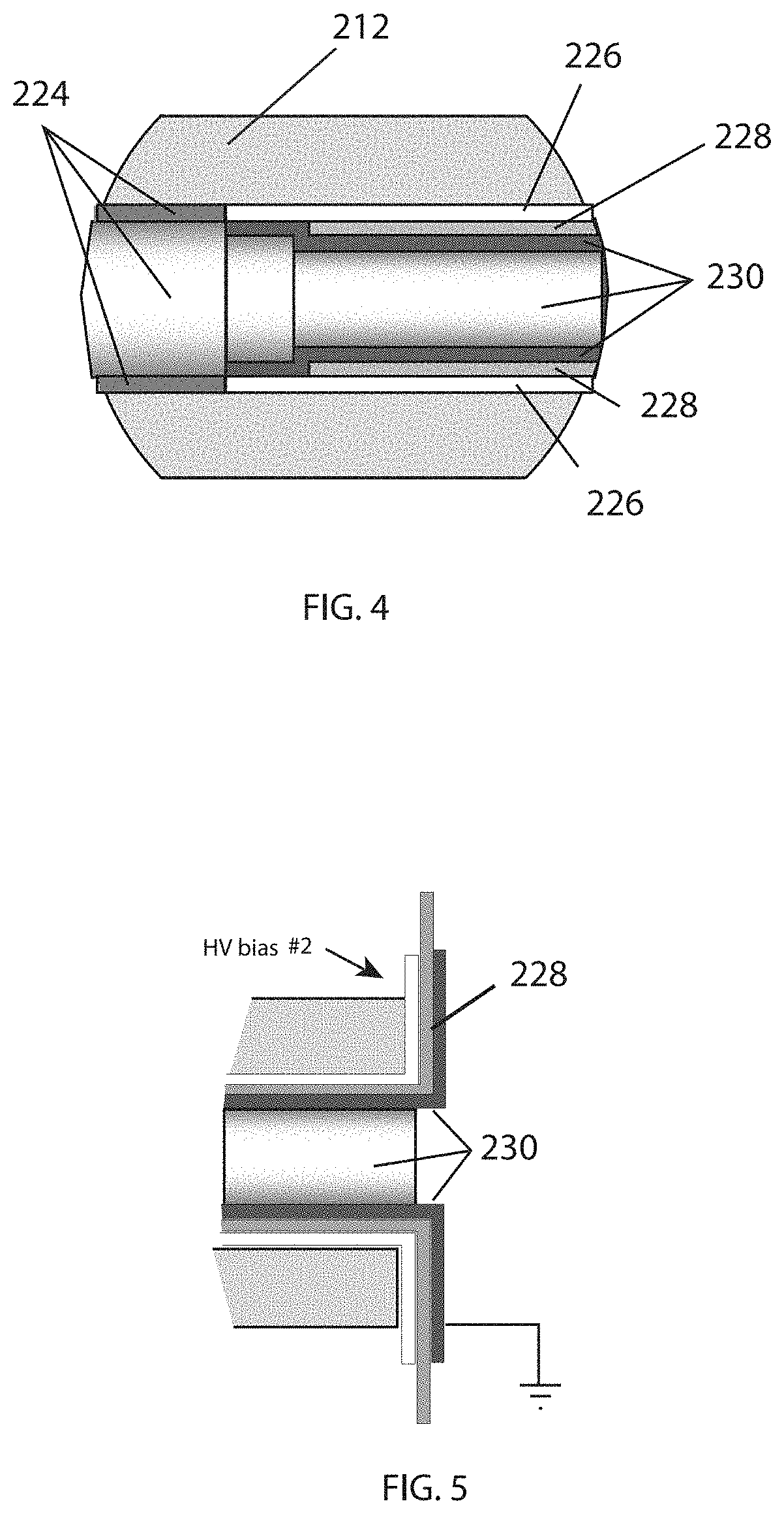
[0022]Shown in FIGS. 3, 4 and 5 is the channel electron multiplier 210 according to the present invention. The channel electron multiplier shown in FIGS. 3, 4, and 5 has all of the features of the channel electron multiplier of FIG. 1 and further includes structure that permits the device to have a second biasing voltage applied. As shown in FIGS. 3, 4, and 5 the channel electron multiplier 210 has a first coating 224 in a first zone (Zone 1) of the internal surface of the elongated tube. In a second zone (Zone 2) of the internal surface, layers of coatings are formed on the internal surface. As shown in FIGS. 4 and 5, a metallic, electrically conductive layer 226 is formed directly on the internal surface of the tube 212. A layer of electrically insulating material 228 is formed on the conductive layer 226 and a layer of electrically resistive material 230 is formed on the electrical insulating layer 228. Preferably, the electrically insulating layer 228 and the electrically resist...


PUM


Abstract

A channel electron multiplier having a high aspect ratio and differential coatings along its channel length is disclosed. The elongated tube has an input end, an output end, and an interior surface extending along the length of the tube between the input end and the output end. The channel electron multiplier also has first and second conductive layers formed on the interior surface of the tube. The first conductive layer is selected to provide a first electrical resistance, a first electron emission characteristic, or both, and the second conductive layer is selected to provide a second electrical resistance, a second electron emission characteristic, or both. A method of making a channel electron multiplier having two or more different conductive layers is also disclosed.

Description

CROSS REFERENCE TO RELATED APPLICATION[0001]This application claims the benefit of U.S. Provisional Patent Application No. 62 / 693,076, filed Jul. 2, 2018, the entirety of which is incorporated by reference herein.BACKGROUND OF THE INVENTIONField of the Invention[0002]This invention relates generally to the formation of coatings on a high aspect ratio object and in particular to a method of forming such coatings by atomic layer deposition to provide two or more coating layers and / or chemistries in different zones along the length of the object. The invention also relates to a channel electron multiplier having two are more resistive coating layers in different zones along the length of the channel electron multiplier. The invention also relates to a channel electron multiplier having one or two or more conducting or insulating layers in different zones along the length of the channel electron multiplier.Description of the Related Art[0003]Electron multipliers have been used as detect...

Claims


Application Information

Patent Timeline
IPC IPC(8): H01J43/06H01J9/24
CPCH01J9/24H01J43/06H01J43/10
Inventor BREUER, MATTHEW
Owner PHOTONIS SCI INC
Why Eureka
Try Eureka