OLED display panel encapsulation structure and OLED display device

a technology of encapsulation structure and oled display panel, which is applied in the field of display, can solve the problems of shortening the product life and oxidation of oled devices, and achieve the effects of reducing the cavities in the organic layer, reducing the risk of oxidation of oled devices, and prolonging the product life of oled devices

Active Publication Date: 2020-01-16
WUHAN CHINA STAR OPTOELECTRONICS SEMICON DISPLAY TECH CO LTD
View PDF5 Cites 1 Cited by
  • Summary
  • Abstract
  • Description
  • Claims
  • Application Information

AI Technical Summary

Benefits of technology

[0005]An object of the present disclosure is to provide an organic light emitting diode (OLED) display panel encapsulation structure to solve issues described above. For example, organic layers may have cavities and water, oxygen and impurities from outer environment may penetrate into the OLED display panel by the cavities to result in a shorter product life and oxidation of OLED device.
[0024]The present invention provides an OLED display panel encapsulation structure. By utilizing the organic layer as an ambipolar layer to decrease the cavities in the organic layer. Thus, the organic layer is able to isolate water and oxygen better and to reduce the risk of oxidation of OLED device and result in longer product life of the OLED device.

Problems solved by technology

For example, organic layers may have cavities and water, oxygen and impurities from outer environment may penetrate into the OLED display panel by the cavities to result in a shorter product life and oxidation of OLED device.

Method used


Image

  • OLED display panel encapsulation structure and OLED display device
  • OLED display panel encapsulation structure and OLED display device

Examples


Embodiment Construction

[0029]The embodiments of the present disclosure are described in detail hereinafter. Examples of the described embodiments are given in the accompanying drawings, wherein the identical or similar reference numerals constantly denote the identical or similar elements or elements having the identical or similar functions. In the description of the present disclosure, it should be understood that terms such as “upper,”“lower,”“front,”“rear,”“left,”“right,”“inside,”“outside,”“lateral,” as well as derivative thereof should be construed to refer to the orientation as then described or as shown in the drawings under discussion. These relative terms are for convenience of description, do not require that the present disclosure be constructed or operated in a particular orientation, and shall not be construed as causing limitations to the present disclosure.

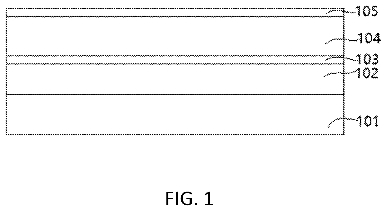
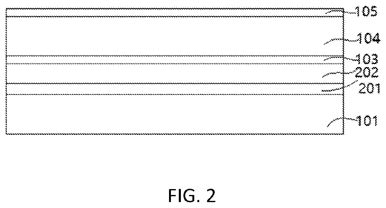
[0030]An object of the present invention is to provide an organic light emitting diode (OLED) display panel encapsulation structure to s...


PUM

PropertyMeasurementUnit
thicknessaaaaaaaaaa
thicknessaaaaaaaaaa
thicknessaaaaaaaaaa

Abstract

An organic light emitting diode (OLED) display panel encapsulation structure includes a first inorganic layer, a first organic layer and a second inorganic layer stacked with one another. The organic layer is an ambipolar layer and the ambipolar layer is made of organic copolymer. Molecules of the organic copolymer have hydrophilic groups and hydrophobic groups. The present invention further provides an OLED display device including a substrate, a thin-film transistor driver layer, an OLED luminescent layer, and an OLED display panel encapsulation structure.

Description

FIELD OF INVENTION[0001]The present invention relates to a display, and more specifically, to an OLED display panel encapsulation structure and an OLED display device having an OLED display panel encapsulation structure.BACKGROUND OF INVENTION[0002]Over the last few years, organic light emitting diodes (OLED) have several advantages such as self-luminescence, quick response times, wide viewing angles, high brightness, light, and thin. Thus, the OLED potential market future is greatly expected.[0003]However, OLED devices are sensitive to water and oxygen. Penetration of water and oxygen greatly negatively influences products lives. That is why effective encapsulating matters. Nowadays, in a conventional OLED display panel encapsulation structure, inorganic layers are hydrophilic and organic layers are hydrophobic. Therefore, during manufacturing of organic layers, the ink for inkjet printing is difficult to flow and spread uniformly on the inorganic layers and easy to form ink drople...

Claims


Application Information

Patent Timeline
Patent Type & Authority Applications(United States)
IPC IPC(8): H01L51/52H01L51/50
CPCH01L51/5256H01L51/5012H10K59/12H10K50/844H10K50/8445H10K50/11
Inventor LI, ZHAO
Owner WUHAN CHINA STAR OPTOELECTRONICS SEMICON DISPLAY TECH CO LTD
Why Eureka
Try Eureka