Image sensor and image capturing apparatus

a technology of image sensor and image capturing apparatus, which is applied in the direction of color television, television system, radio frequency control device, etc., can solve the problems of carrier inability to accelerate, and the reduction in the efficiency of incident photon detection, so as to suppress the reduction in the efficiency of photon detection

Active Publication Date: 2020-01-16
CANON KK
View PDF0 Cites 3 Cited by
  • Summary
  • Abstract
  • Description
  • Claims
  • Application Information

AI Technical Summary

Benefits of technology

[0007]The present invention has been made in view of the aforementioned problems with conventional techniques. The present invention provide

Problems solved by technology

This gives rise to the possibility that carriers cannot be accelerated to the speed that is necessary for avalanche breakdown to occur in the high-field region.
Furthermore, in a pixel in which carriers move a long dist

Method used


Image

  • Image sensor and image capturing apparatus
  • Image sensor and image capturing apparatus
  • Image sensor and image capturing apparatus

Examples


first embodiment

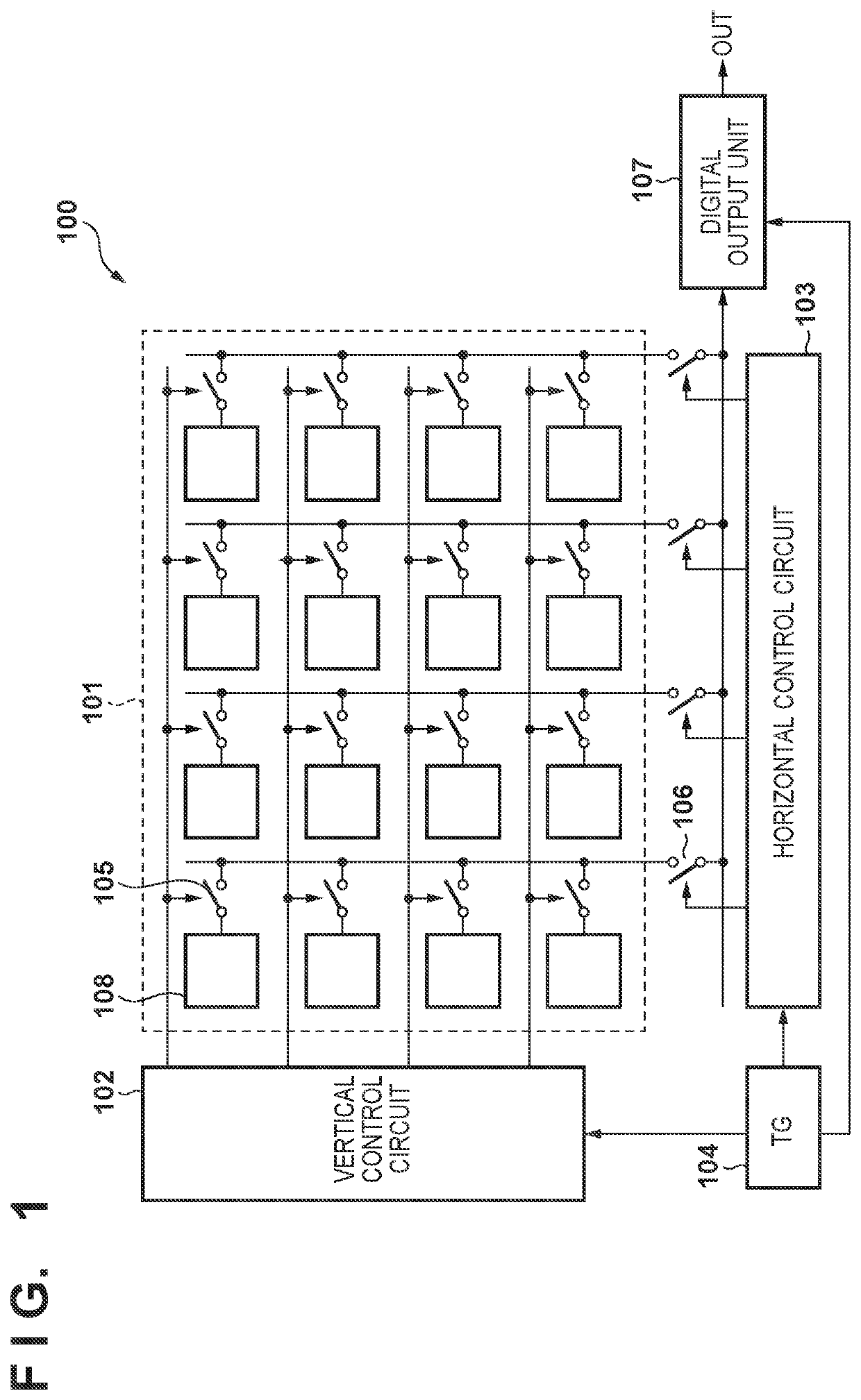
[0026]FIG. 1 schematically shows an exemplary configuration of an image sensor according to an embodiment of the present invention. An image sensor 100 includes a pixel region 101, a vertical control circuit 102, a horizontal control circuit 103, a timing generator (TG) 104, and a digital output unit 107.

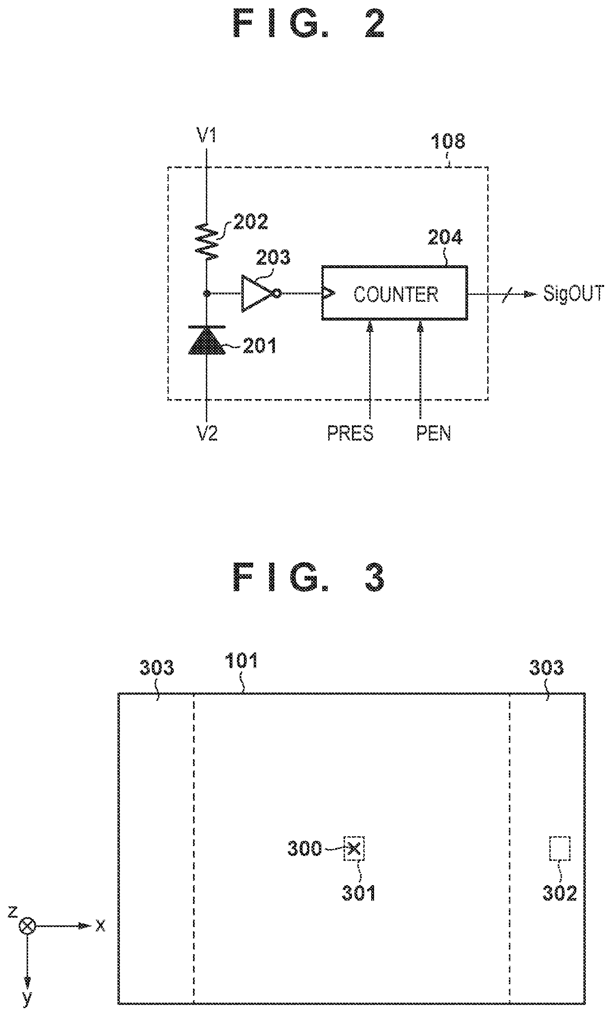
[0027]In the pixel region 101, a plurality of pixels 108 are arranged in a matrix. Although four pixels are arrayed in a horizontal direction and four pixels are arrayed in a vertical direction in the illustrated pixel region 101 for ease of explanation, a large number of pixels, such as several millions to tens of millions of pixels, are arrayed in reality. The pixels 108 count pulse signals attributed to incident photons, and output a counted value in a digital form as pixel data. The specifics of these pixels will be described later using FIG. 2.

[0028]The vertical control circuit 102 selects pixels 108 on a row-by-row basis using switches 105. The vertical control circuit 102 als...

second embodiment

[0074]Next, a second embodiment of the present invention will be described. In the present embodiment, the present invention is applied to pixels that are configured to include a microlens and a light-receiving region divided into a plurality of regions. FIG. 8 is an equivalent circuit diagram of pixels 108′ that are arrayed in a pixel region of an image sensor of the present embodiment. The constituent elements that are similar to those of the pixels 108 in the first embodiment will be given the same reference signs as in FIG. 2, and a description thereof will be omitted.

[0075]The pixels 108′ included in the image sensor of the present embodiment include a plurality of photodiodes 201A, 201B. Note that each pixel may include three or more photodiodes. The pixels 108′ also include quenching resistors 202A, 202B, inverting buffers 203A, 203B, and counter circuits 204A, 204B that respectively correspond to the photodiodes 201A, 201B.

[0076]A voltage V1_A (e.g., 3 V) is applied to a cat...

third embodiment

[0090]Next, a third embodiment of the present invention will be described. In the present embodiment, the present invention is applied to pixels that are configured to include a microlens and a light-shielding film that blocks light from entering a part of a light-receiving region. An equivalent circuit of the pixels included in an image sensor according to the present embodiment is similar to that of the first embodiment (FIG. 2).

[0091]The following describes the embodiment in which, in one or more of pixels in an imaging region, focus detection according to a phase-difference detection method can be performed by blocking a part of a light beam incident on a photodiode via the microlens using the light-shielding film.

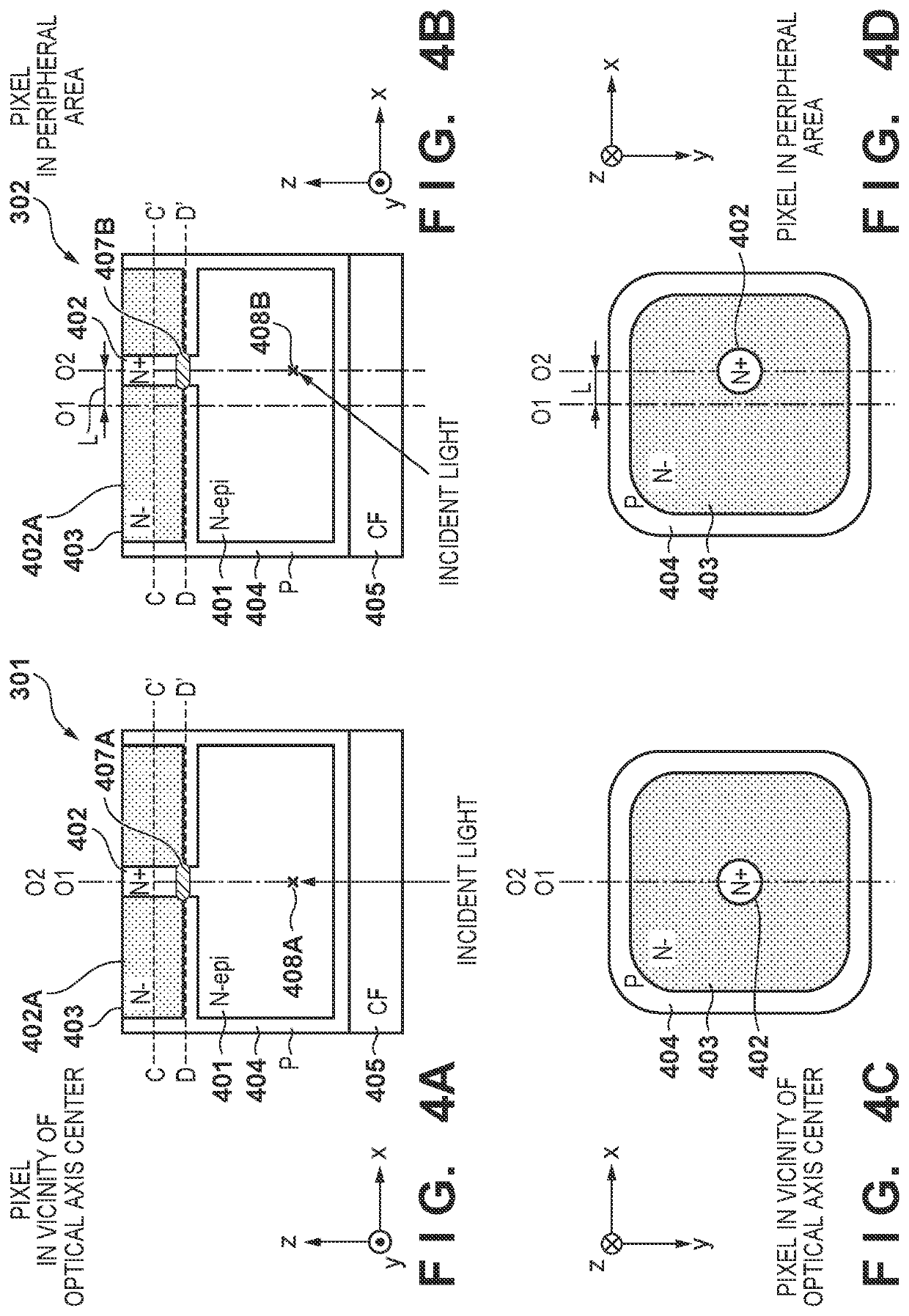
[0092]FIG. 10A is a schematic view of a pixel region 101 of the image sensor according to the present embodiment, and the constituent elements that are similar to those of the first embodiment are given the same reference signs as in FIG. 3. In the present embodiment a...


PUM


Abstract

An image sensor of a photon counting type that suppresses a reduction in the efficiency of photon detection dependent on a pixel position, is disclosed. The image sensor comprising a pixel region in which a plurality of pixels are arrayed in a matrix, each pixel including a photoelectric conversion region and an avalanche breakdown region. In a plan view of a pixel, a size of the avalanche breakdown region is smaller than a size of the photoelectric conversion region. In addition, at least some of pixels arranged in a peripheral region of the pixel region, the avalanche breakdown region is formed such that a position thereof is shifted with respect to a position of the avalanche breakdown region in pixels arranged in a central region of the pixel region.

Description

BACKGROUND OF THE INVENTIONField of the Invention[0001]The present invention relates to an image sensor and an image capturing apparatus, and in particular to a structure of an image sensor.Description of the Related Art[0002]A photodiode array has been suggested that includes an array of avalanche photodiodes (APDs) to which a reverse bias voltage higher than a breakdown voltage has been applied, and that detects the number of photons incident on a certain range (Japanese Patent Laid-Open No. 2012-174783). The use of such a photodiode array as an image sensor of a photon counting type has also been suggested.[0003]APDs to which a reverse bias voltage higher than a breakdown voltage has been applied generate a light current through avalanche breakdown each time photons are incident. The number of photons incident on the APDs can be detected by shaping voltage changes associated with the generation of the light current into pulse signals and counting the generated pulse signals using...

Claims


Application Information

Patent Timeline
IPC IPC(8): H04N5/3745H01L27/146H01L31/107H04N5/378
CPCH01L31/107H01L27/1461H01L27/14621H04N5/3745H01L27/14627H04N5/378H01L27/14623H04N23/54H04N25/70H01L27/1464H01L27/14605H01L31/035272H04N25/77H04N25/75
Inventor IKEDO, HIDEKIKOBAYASHI, HIROKAZU
Owner CANON KK
Why Eureka
Try Eureka