Semiconductor device and electronic device

a technology of semiconductor devices and electronic devices, applied in pulse generators, pulse techniques, instruments, etc., can solve the problems of increasing the number of circuits included in a chip, increasing the power consumption and heat generated during the driving of a device, and achieves low power consumption, increased power consumption and heat generated. , the effect of not easily affected by environmental temperatur

Active Publication Date: 2020-01-23
SEMICON ENERGY LAB CO LTD
View PDF0 Cites 4 Cited by
  • Summary
  • Abstract
  • Description
  • Claims
  • Application Information

AI Technical Summary

Benefits of technology

[0010]An increase in the number of circuits included in a chip increases the power consumption and the amount of heat generated during the driving of a device. In particular, a larger amount of heat generation is more likely to affect the characteristics of circuit components included in a chip; thus, the circuit components included in the chip are preferably less affected by temperatures.
[0011]An object of one embodiment of the present invention is to provide a semiconductor device or the like including a hierarchical artificial neural network. Another object of one embodiment of the present invention is to provide a semiconductor device or the like with low power consumption. Another object of one embodiment of the present invention is to provide a semiconductor device or the like that is not easily affected by environmental temperature. Another object of one embodiment of the present invention is to provide a novel semiconductor device or the like.

Problems solved by technology

An increase in the number of circuits included in a chip increases the power consumption and the amount of heat generated during the driving of a device.

Method used


Image

  • Semiconductor device and electronic device
  • Semiconductor device and electronic device
  • Semiconductor device and electronic device

Examples


embodiment 1

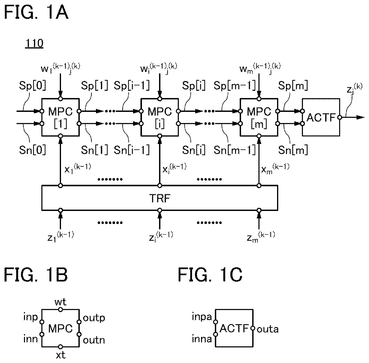
[0112]In this embodiment, an arithmetic circuit that is a semiconductor device of one embodiment of the present invention and performs neural network operation will be described.

[0113]First, a hierarchical neural network is described. A hierarchical neural network includes three or more layers of one input layer, one or more intermediate layers (hidden layers), and one output layer, for example. FIG. 4A illustrates an example of the hierarchical neural network, and a neural network 100 includes first to R-th layers (here, R is an integer greater than or equal to 4). Specifically, the first layer is the input layer, the R-th layer is the output layer, and the other layers are the intermediate layers. Note that FIG. 4A illustrates the (k−1)th layer and the k-th layer (here, k is an integer greater than or equal to 3 and less than or equal to R−1) as the intermediate layers, and does not show the other intermediate layers.

[0114]Each of the layers of the neural network 100 includes one ...

embodiment 2

[0248]In this embodiment, another configuration example of the arithmetic circuit 110 shown in Embodiment 1 will be described.

110>

[0249]In the arithmetic circuit 110 in FIG. 1A, the circuits MPC can be arranged in a matrix, for example. FIG. 9 illustrates a configuration example of such an arithmetic circuit.

[0250]An arithmetic circuit 120 includes an array portion ALP including the circuits MPC arranged in a matrix, a circuit AFP including a plurality of circuits ACTF, a circuit TSG, a circuit WLD, a circuit SWLD, and the converter circuit TRF.

[0251]The array portion ALP includes n×m circuits MPC, and the circuits MPC are arranged in a matrix of n rows and m columns in the array portion ALP. Note that in FIG. 9, a circuit MPC[j, i] represents the circuit MPC in the j-th row and the i-th column (here, j is an integer greater than or equal to 1 and less than or equal to n, and i is an integer greater than or equal to 1 and less than or equal to m). Note that FIG. 9 illustrates only c...

embodiment 3

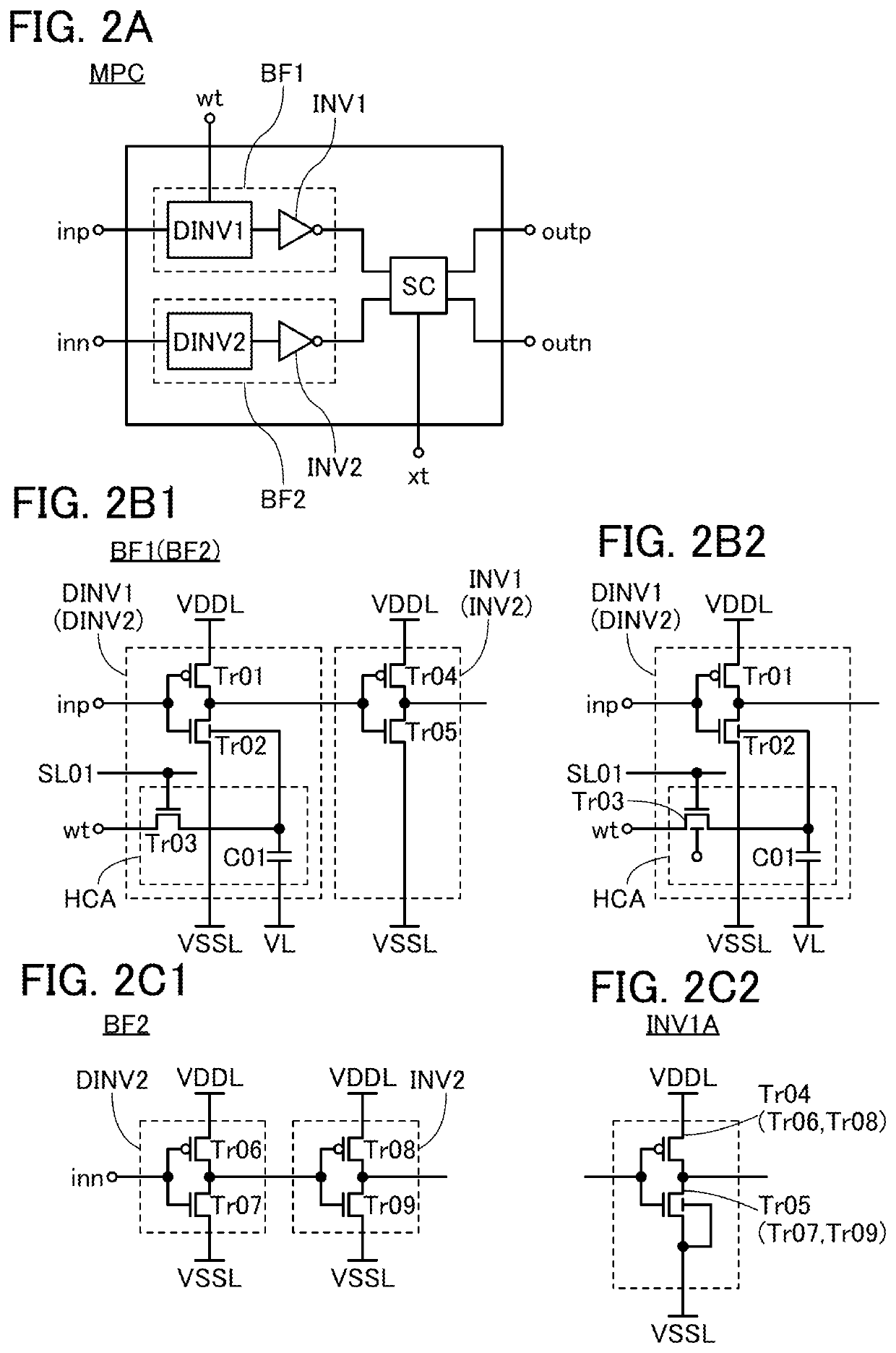
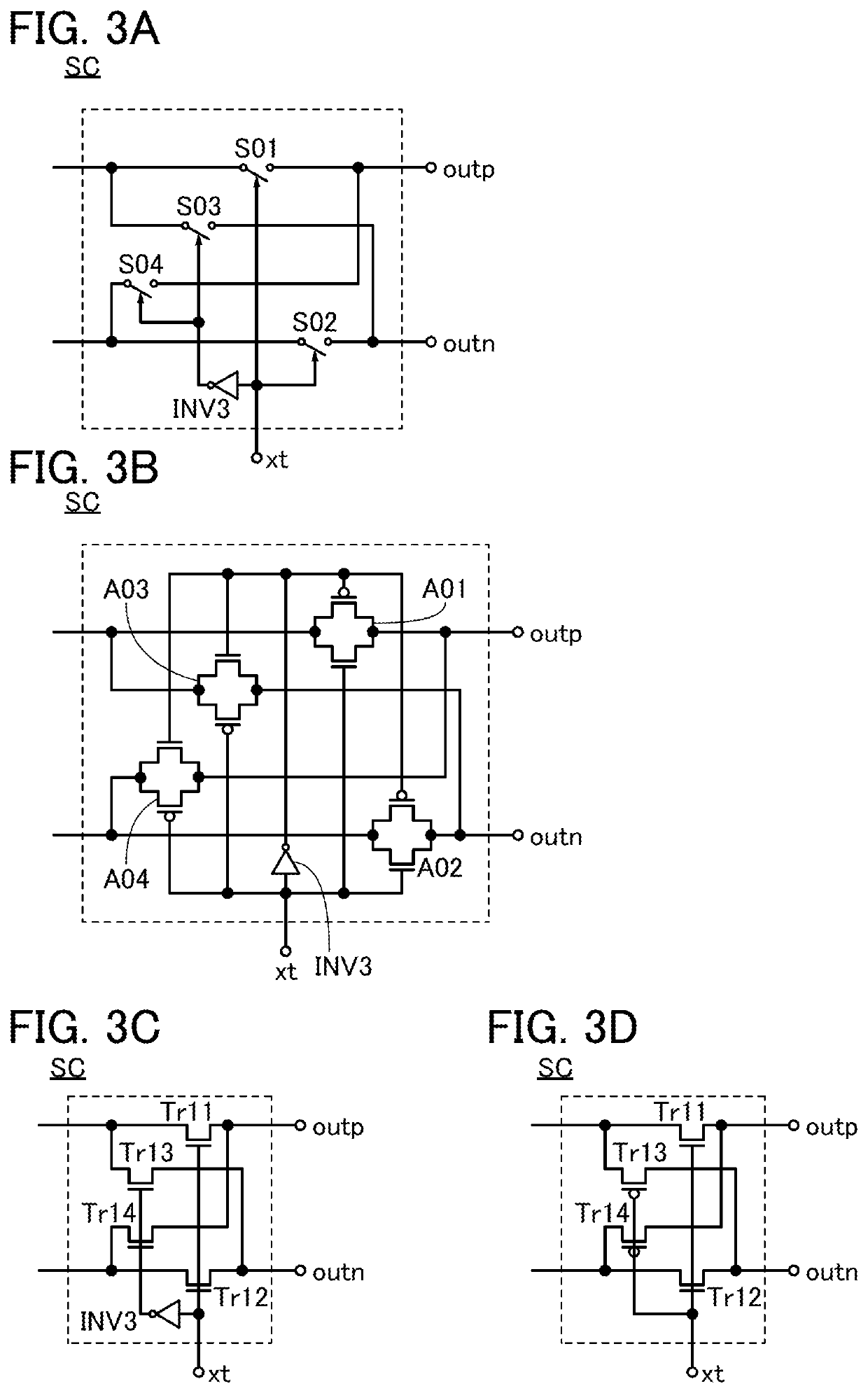
[0270]In this embodiment, other configuration examples of the circuit MPC shown in Embodiment 1 will be described.

[0271]The circuit MPC illustrated in FIG. 12A includes a circuit SDINV, an inverter circuit INV7, and an inverter circuit INV8.

[0272]The circuit SDINV includes two input terminals and two output terminals. One of the two input terminals of the circuit SDINV is electrically connected to the terminal inp, and the other of the two input terminals of the circuit SDINV is electrically connected to the terminal inn. One of the two output terminals of the circuit SDINV is electrically connected to an input terminal of the inverter circuit INV7, and the other of the two output terminals of the circuit SDINV is electrically connected to an input terminal of the inverter circuit INV8. An output terminal of the inverter circuit INV7 is electrically connected to the terminal outp, and an output terminal of the inverter circuit INV8 is electrically connected to the terminal outn. The...


PUM

PropertyMeasurementUnit
time lagaaaaaaaaaa
resistanceaaaaaaaaaa
resistancesaaaaaaaaaa

Abstract

A semiconductor device capable of performing product-sum operation with low power consumption. The semiconductor device includes first and second logic circuits, first to fourth transistors, and first and second holding units. A low power supply potential input terminal of the first logic circuit is electrically connected to the first and third transistors. A low power supply potential input terminal of the second logic circuit is electrically connected to the second and fourth transistors. The potentials of second gates of the first and fourth transistors are held in the first holding unit as potentials corresponding to first data. The potentials of second gates of the second and third transistors are held in the second holding unit. The on/off states of the first to fourth transistors are determined by second data. A difference in signal input/output time between the first and second logic circuits depends on the first data and the second data.

Description

BACKGROUND OF THE INVENTION1. Field of the Invention[0001]One embodiment of the present invention relates to a semiconductor device and an electronic device.[0002]Note that one embodiment of the present invention is not limited to the above technical field. The technical field of the invention disclosed in this specification and the like relates to an object, a method, or a manufacturing method. In addition, one embodiment of the present invention relates to a process, a machine, manufacture, or a composition of matter. Specific examples of the technical field of one embodiment of the present invention disclosed in this specification include a semiconductor device, a display device, a liquid crystal display device, a light-emitting device, a power storage device, an imaging device, a memory device, a signal processing device, a processor, an electronic device, a system, a method for driving any of them, a method for manufacturing any of them, and a method for inspecting any of them....

Claims


Application Information

Patent Timeline
Patent Type & Authority Applications(United States)
IPC IPC(8): H03K3/037G11C13/00G11C11/16G06N3/04
CPCG11C11/16G11C13/0004H03K3/037G06N3/04G11C7/1006G11C11/54G11C11/1659G11C13/003G11C2029/5002G11C2029/0403G06N3/065G06N3/048
Inventor KIMURA, HAJIMEKUROKAWA, YOSHIYUKI
Owner SEMICON ENERGY LAB CO LTD
Why Eureka
Try Eureka